SBVS441 December 2022 TPS7B4255
PRODUCTION DATA
- 1 Features
- 2 Applications
- 3 Description
- 4 Revision History
- 5 Pin Configuration and Functions
- 6 Specifications
- 7 Detailed Description
- 8 Application and Implementation
- 9 Device and Documentation Support
- 10Mechanical, Packaging, and Orderable Information
Package Options
Mechanical Data (Package|Pins)
- DBV|5
Thermal pad, mechanical data (Package|Pins)
Orderable Information
8.4.1.4 Thermal Performance Versus Copper Area
The most used thermal resistance parameter RθJA is highly dependent on the heat-spreading capability built into the particular PCB design, and therefore varies according to the total copper area, copper weight, and location of the planes. The RθJA recorded in the Section 6.4 table is determined by the JEDEC standard (Figure 8-7), PCB, and copper-spreading area, and is only used as a relative measure of package thermal performance. For a well-designed thermal layout, RθJA is actually the sum of the package junction-to-case (bottom) thermal resistance (RθJCbot) plus the thermal resistance contribution by the PCB copper.
 Figure 8-7 JEDEC Standard 2s2p
PCB
Figure 8-7 JEDEC Standard 2s2p
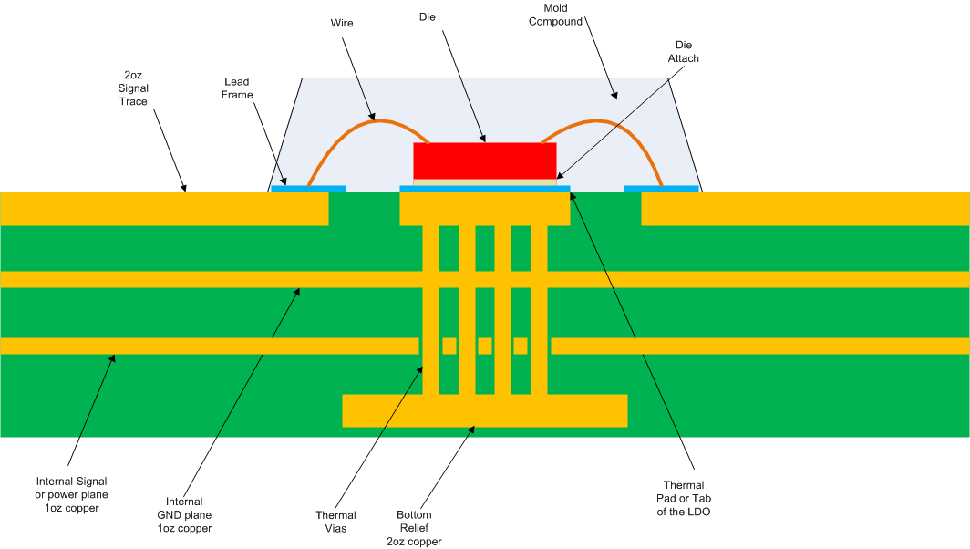
PCBFigure 8-8 and Figure 8-9 illustrate the functions of RθJA and ψJB versus copper area and thickness. These plots are generated with a 101.6-mm × 101.6-mm × 1.6-mm PCB of two and four layers. For the 4-layer board, inner planes use 1-oz copper thickness. Outer layers are simulated with both 1-oz and 2-oz copper thickness. A 4 x 5 (DBV package) array of thermal vias with a 300-µm drill diameter and 25-µm copper plating is located as close as practical to the GND pin of the device. The thermal vias connect the top layer, the bottom layer and, in the case of the 4-layer board, the first inner GND plane. Each of the layers has a copper plane of equal area.
As illustrated in Figure 8-9, ψJB increases with increasing connecting copper area. The reason for this increase is that the board temperature is measured at the copper near the GND pin, and because the GND pin is fused to the die pad, more heat escapes through the GND pin when more copper is connected to the pad, and thus the temperature at this point is higher. Consequently the ψJB increases. This increase does not imply that heat sinking for the device is reduced when more connecting copper is added. Increasing connecting copper area always increases board-level heat sinking for the device. Furthermore, the boards used for Figure 8-9 have vias connecting to internal copper planes. Therefore, ψJB is much higher than what is specified in the Section 6.4 table, which uses the high-K board layout specified in JESD51-7 that has no thermal vias.