SNVS900B DECEMBER 2012 – December 2015 TPS92560
PRODUCTION DATA.
- 1 Features
- 2 Applications
- 3 Description
- 4 Revision History
- 5 Pin Configuration and Functions
- 6 Specifications
- 7 Detailed Description
- 8 Application and Implementation
- 9 Power Supply Recommendations
- 10Layout
- 11Device and Documentation Support
- 12Mechanical, Packaging, and Orderable Information
Package Options
Mechanical Data (Package|Pins)
- DGQ|10
Thermal pad, mechanical data (Package|Pins)
- DGQ|10
Orderable Information
1 Features
- Controlled peak input current to prevent over-stressing of the electronic transformer
- Allows Either Step-Up or Step-Up/Down Operation
- Compatible to Generic Electronic Transformers
- Compatible to Magnetic Transformers and DC Power Supplies
- Integrated Active Low-Side Input Rectifiers
- Compact and Simple Circuit
- >85% Dfficiency (12-VDC Input)
- Power Factor > 0.9 (Full Load With AC input)
- Hysteretic Control Scheme
- Output Overvoltage Protection
- Overtemperature Shutdown
- 10-pin Thermally Enhanced Very-Thin Fine Pitch Small-Outline Package
2 Applications
- MR16/AR111 LED Lamps
- Lighting System Using Electronic Transformer
- General Lighting Systems That Require a Boost / SEPIC LED Driver
3 Description
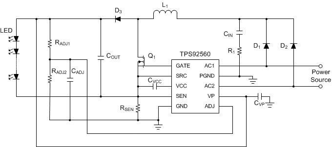
The TPS92560 is a simple LED driver designed to drive high-power LEDs by drawing constant current from the power source. The device is ideal for MR16 and AR111 applications, which require good compatibility to DC and AC voltages and electronic transformers. The hysteretic control scheme does not need control loop compensation while providing the benefits of fast transient response and high power factor. The patent pending feedback control method allows the output power to be determined by the number of LED used without component change. The TPS92560 supports both boost and SEPIC configurations for the use of different LED modules.
Device Information(1)
| PART NUMBER | PACKAGE | BODY SIZE (NOM) |
|---|---|---|
| TPS92560 | HVSSOP (10) | 3.00 mm × 3.00 mm |
- For all available packages, see the orderable addendum at the end of the data sheet.
Typical Application Schematic
