SNVS900B DECEMBER 2012 – December 2015 TPS92560
PRODUCTION DATA.
- 1 Features
- 2 Applications
- 3 Description
- 4 Revision History
- 5 Pin Configuration and Functions
- 6 Specifications
- 7 Detailed Description
- 8 Application and Implementation
- 9 Power Supply Recommendations
- 10Layout
- 11Device and Documentation Support
- 12Mechanical, Packaging, and Orderable Information
Package Options
Mechanical Data (Package|Pins)
- DGQ|10
Thermal pad, mechanical data (Package|Pins)
- DGQ|10
Orderable Information
7 Detailed Description
7.1 Overview
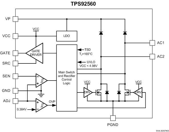
The TPS92560 is a simple hysteretic control switching LED driver for MR16 or AR111 lighting applications. The device accepts DC voltage, AC voltage and electronic transformer as an input power source. The compact application circuit can fit into a generic case of MR16 lamps easily. The hysteretic inductor current control scheme requires no small signal control loop compensation and maintains constant average input current to secure high compatibility to different kinds of input power source. The TPS92560 can be configured to either a step-up or step-up/down LED driver for the use of different number of LEDs. The patent pending current control mechanism allows the use of a single set of component and PCB layout for serving different output power requirements by changing the number of LEDs. The integrating of the active low-side input rectifiers reduces the power loss for voltage rectification and saves two external diodes of a generic bridge rectifier to aim for a simple end application circuit. When the driver is used with an AC voltage source or electronic transformer, the current regulation level increases accordingly to maintain an output current close to the level that when it is used with a DC voltage source. With the output overvoltage protection and over-temperature shutdown functions, the TPS92560 is specifically suitable for the applications that are space limited and need wide acceptance to different power sources.
7.2 Functional Block Diagram

7.3 Feature Description
7.3.1 VCC Regulator
The VCC pin is the output of the internal linear regulator for providing an 8.45V typical supply voltage to the MOSFET driver and internal circuits. The output current of the VCC pin is limited to 30mA typical. A low ESR ceramic capacitor of 0.47-μF or higher capacitance should be connected across the VCC and SRC pins to supply transient current to the MOSFET driver.
7.3.2 MOSFET Driver
The GATE pin is the output of the gate driver which referenced to the SRC pin. The gate driver is powered directly by the VCC regulator which the maximum gate driving current is limited to 30 mA (typical). To prevent hitting the VCC current limit, TI suggests using a low gate charge MOSFET when high switching frequency is needed.
7.3.3 ADJ Pin
The voltage on the ADJ pin determines the reference voltage for the input current regulation. Typically, the ADJ pin voltage is divided from the output voltage of the circuit by a voltage divider, thus the average input current is adjusted with respect to the number of LEDs used. The voltage of the ADJ pin determines the input current following the expression:

7.3.3.1 Output OVP
In the TPS92560, a function of output overvoltage protection (OVP) is provided to prevent damaging the circuit due to an open circuit of the LED. The OVP function is implemented to the ADJ pin. When the voltage of the ADJ pin exceeds 0.384V typical, the OVP circuit disables the MOSFET driver and turns off the main switch to allow the output capacitor to discharge. As the voltage of the ADJ pin decreases to below 0.353 V (typical), the MOSFET driver is enabled and the TPS92560 returns to normal operation. The triggering threshold of the output voltage is determined by the value of the resistors RADJ1 and RADJ2, which can be calculated using the following equation:

When defining the OVP threshold voltage, it is necessary to certain that the OVP threshold voltage does not exceed the rated voltage of the output rectifier and capacitor to avoid damaging of the circuit.
7.3.4 AC1 and AC2 Pins
The TPS92560 provides two internal active rectifiers for input voltage rectification. Each internal rectifier connects across the ACn pin to GND. These internal active rectifiers function as the low-side diode rectifiers of a generic bridge rectifier. The integrating of the active rectifiers helps in saving two external diodes of a bridge rectifier along with an improvement of power efficiency. For high power applications, for instance, 12-W output power, external diode rectifiers can be added across the ACn pin to GND to reduce heat dissipation on the TPS92560.
7.3.5 Detection of Power Source
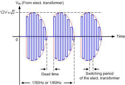
 Figure 13. Inherent Dead Time of the Output Voltage of an Electronic Transformer
Both the voltages of a generic AC source (50/60Hz) and an electronic transformer carry certain amount of dead time inherently, as shown in Figure 13. The existing of the dead time leads to a drop of the RMS input power to the driver circuit. In order to compensate the drop of the RMS input power, the ADJ pin sources current to the resistor, RADJ2 to increase the reference voltage for the current regulation loop and in turn increase the RMS input power accordingly when an AC voltage source or electronic transformer is detected. The output current of the ADJ pin for an AC input voltage and electronic transformer are 9.5μA and 11.5μA typical respectively. Practically the amount of the power for compensating the dead time of the input power source differs case to case depending on the characteristics of the power source, the value of the RADJ1 and RADJ2 might need a fine adjustment in accordance to the characteristics of the power source. The additional output power for compensating the dead time of the power sources (ΔPLED) are calculated using the following Equation 3 and Equation 4.
For 50/60Hz AC power source:

For electronic transformer:

7.3.6 Current Regulation
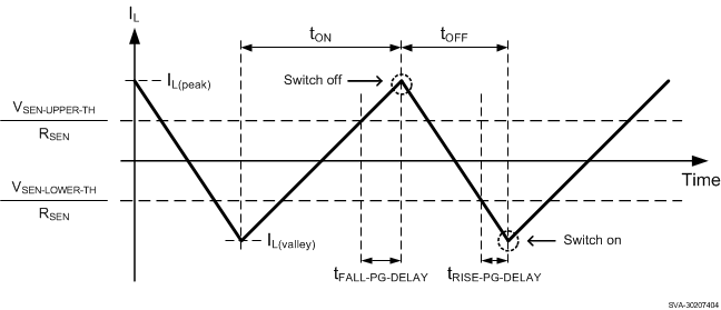
In the TPS92560, the input current regulation is attained by limiting the peak and valley of the inductor current. Practically the inductor current sensing is facilitated by detecting the voltage on the resistor, RSEN. Because the current flows through the RSEN is a sum total of the currents of the main switch and LEDs, the voltage drop on the RSEN reflects the current of the inductor that is identical to the input current to the LED driver circuit. Figure 14 shows the waveform of the inductor current ripple with the peak and valley values controlled.
 Figure 14. Inductor Current Ripple in Steady State
The voltage of the ADJ pin is determined by the forward voltage of the LED and divided from the VVP by a resistor divider. The equation for calculating the VADJ as shown in Equation 5.

In steady state, the voltage drop on the RADJ1 is identical to the forward voltage of the LED (VLED) and the voltage across the RADJ2 is identical to the voltage across the RSEN. The LED current, ILED is then calculated following the equations:
In steady state:


Since

Thus,

Put the expressions (2) to (4) into (5):

Due to the high input impedance of the ADJ pin, the current flows into the ADJ pin can be neglected and thus IRADJ1 equals IRADJ2. The LED current is then calculated following the expressions below:

Practically, the conversion efficiency of a boost circuit is almost a constant around 85%. Being assumed that the efficiency term in the ILED expression is a constant, the LED current depends solely on the magnitude of the input voltage, VIN. Without changing a component, the output power of the typical application circuits of the TPS92560 is adjustable by using different number of LEDs.
The output power is calculated by following the expression:

7.3.7 Switching Frequency (Boost Configuration)
In the following sections, the equations and calculations are limited to the boost configuration only (that is, the LED forward voltage higher than the input voltage), unless otherwise specified. The application information for the SEPIC and other circuit topologies are available in separate application notes and reference designs. In the boost configuration, including the propagation delay of the control circuit, the ON and OFF times of the main switch are calculated using Equation 14 and Equation 15.


In the previous equations, the VD is the forward voltage of D3, RL is the DC resistance of L1, RDS(ON) is the ON resistance of Q1 and RAC-FET is the turn ON resistance of the internal active rectifier with respect to the typical application circuit diagram.
Practically the resistance of the RL, RDS(on) and RAC-FET is in the order if several tenth of mΩ, by assuming a 0.5-V diode forward voltage and the sum total of the RL, RDS(ON) and RAC-FET is close to 1 Ω, the on and off times of Q1 can be approximated using the Equation 16 and Equation 17.


With the switching on and OF times determined, the switching frequency can be calculated using Equation 18.

Because of the using of hysteretic control scheme, the switching frequency of the TPS92560 in steady state is dependent on the input voltage, output voltage and inductance of the inductor. Generally a 1-MHz to 1.5-MHz switching frequency is suggested for applications using an electronic transformer as the power source.
7.3.8 Inductor Selection (Boost Configuration)
Because of the using of the hysteretic control scheme, the switching frequency of the TPS92560 in a boost configuration can be adjusted in accordance to the value of the inductor being used. Derived from the equations (12) and (13), the value of the inductor can be determined base on the desired switching frequence by using Equation 19.

When selecting the inductor, it is essential to ensure the peak inductor current does not exceed the the factory suggested saturation current of the inductor. The values of the peak and valley inductor current are calculated using the following equations:
Peak inductor current:

Valley inductor current:

Assume the total resistance of the RL, RDS(on) and RAC-FET is 1 Ω and the diode drop, VD equal to 1 V, the peak and valley currents of the inductor can be approximated using Equation 22 and Equation 23.


In order not to saturate the inductor, an inductor with a factory guranteed saturation current (ISAT) 20% higher than the IL(peak) is suggested. Thus the ISAT of the inductor should fulfill the following requirement:

7.3.9 Input Surge Voltage Protection
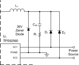
When use with an electronic transformer, the surge voltage across the input terminals can be sufficiently high to damage the TPS92560 depending on the characteristics of the electronic transformer. To against potential damaging due to the input surge voltage, a 36-V Zener diode can be connected across the input bridge rectifier as shown in Figure 15.
 Figure 15. Input Surge Voltage Protection Using an External Zener Diode
7.4 Device Functional Modes
7.4.1 Thermal Shutdown
The TPS92560 includes a thermal shutdown circuitry that ceases the operation of the device to avoid permanent damage. The threshold for thermal shutdown is 165°C with a 30°C hysteresis typical. During thermal shutdown the VCC regulator is disabled and the MOSFET is turned off.