SLDS238B January   2018  – January  2020 TPS92611-Q1

PRODUCTION DATA.  

  1. Features
  2. Applications
  3. Description
    1.     Typical Application Diagram
  4. Revision History
  5. Pin Configuration and Functions
    1.     Pin Functions
  6. Specifications
    1. 6.1 Absolute Maximum Ratings
    2. 6.2 ESD Ratings
    3. 6.3 Recommended Operating Conditions
    4. 6.4 Thermal Information
    5. 6.5 Electrical Characteristics
    6. 6.6 Timing Requirements
    7. 6.7 Typical Characteristics
  7. Detailed Description
    1. 7.1 Overview
    2. 7.2 Functional Block Diagram
    3. 7.3 Feature Description
      1. 7.3.1 Device Bias
        1. 7.3.1.1 Power-On Reset (POR)
        2. 7.3.1.2 Low-Quiescent-Current Fault Mode
      2. 7.3.2 Constant-Current Driver
      3. 7.3.3 Device Enable
      4. 7.3.4 PWM Dimming
      5. 7.3.5 Diagnostics
        1. 7.3.5.1 DIAGEN
        2. 7.3.5.2 Low-Dropout Mode
        3. 7.3.5.3 Open-Circuit Detection
        4. 7.3.5.4 Short-to-GND Detection
        5. 7.3.5.5 Overtemperature Protection
      6. 7.3.6 Fault-Bus Output With One-Fails–All-Fail
    4. 7.4 Device Functional Modes
      1. 7.4.1 Undervoltage Lockout, V(SUPPLY) < V(POR_rising)
      2. 7.4.2 Normal Operation V(SUPPLY) ≥ 4.5 V
      3. 7.4.3 Low-Voltage Dropout
      4. 7.4.4 Fault Mode
  8. Application and Implementation
    1. 8.1 Application Information
    2. 8.2 Typical Application
      1. 8.2.1 Single-Channel LED Driver With Diagnostics
        1. 8.2.1.1 Design Requirements
        2. 8.2.1.2 Detailed Design Procedure
        3. 8.2.1.3 Application Curve
      2. 8.2.2 Single-Channel LED Driver With Heat Sharing
        1. 8.2.2.1 Design Requirements
        2. 8.2.2.2 Detailed Design Procedure
        3. 8.2.2.3 Application Curve
  9. Power Supply Recommendations
  10. 10Layout
    1. 10.1 Layout Guidelines
    2. 10.2 Layout Example
  11. 11Device and Documentation Support
    1. 11.1 Documentation Support
      1. 11.1.1 Related Documentation
    2. 11.2 Receiving Notification of Documentation Updates
    3. 11.3 Community Resources
    4. 11.4 Trademarks
    5. 11.5 Electrostatic Discharge Caution
    6. 11.6 Glossary
  12. 12Mechanical, Packaging, and Orderable Information

Package Options

Mechanical Data (Package|Pins)
Thermal pad, mechanical data (Package|Pins)
Orderable Information

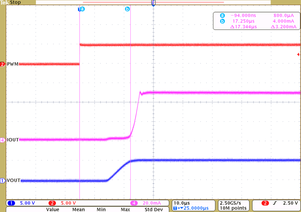
Application Curve

TPS92611-Q1 app-diagnostics-curve-slds233.png
Ch. 1 = V(OUT) Ch. 2 = V(PWM) Ch. 4 = I(OUT)
Figure 20. Output Current With PWM Input