SLDS238B January   2018  – January  2020 TPS92611-Q1

PRODUCTION DATA.  

  1. Features
  2. Applications
  3. Description
    1.     Typical Application Diagram
  4. Revision History
  5. Pin Configuration and Functions
    1.     Pin Functions
  6. Specifications
    1. 6.1 Absolute Maximum Ratings
    2. 6.2 ESD Ratings
    3. 6.3 Recommended Operating Conditions
    4. 6.4 Thermal Information
    5. 6.5 Electrical Characteristics
    6. 6.6 Timing Requirements
    7. 6.7 Typical Characteristics
  7. Detailed Description
    1. 7.1 Overview
    2. 7.2 Functional Block Diagram
    3. 7.3 Feature Description
      1. 7.3.1 Device Bias
        1. 7.3.1.1 Power-On Reset (POR)
        2. 7.3.1.2 Low-Quiescent-Current Fault Mode
      2. 7.3.2 Constant-Current Driver
      3. 7.3.3 Device Enable
      4. 7.3.4 PWM Dimming
      5. 7.3.5 Diagnostics
        1. 7.3.5.1 DIAGEN
        2. 7.3.5.2 Low-Dropout Mode
        3. 7.3.5.3 Open-Circuit Detection
        4. 7.3.5.4 Short-to-GND Detection
        5. 7.3.5.5 Overtemperature Protection
      6. 7.3.6 Fault-Bus Output With One-Fails–All-Fail
    4. 7.4 Device Functional Modes
      1. 7.4.1 Undervoltage Lockout, V(SUPPLY) < V(POR_rising)
      2. 7.4.2 Normal Operation V(SUPPLY) ≥ 4.5 V
      3. 7.4.3 Low-Voltage Dropout
      4. 7.4.4 Fault Mode
  8. Application and Implementation
    1. 8.1 Application Information
    2. 8.2 Typical Application
      1. 8.2.1 Single-Channel LED Driver With Diagnostics
        1. 8.2.1.1 Design Requirements
        2. 8.2.1.2 Detailed Design Procedure
        3. 8.2.1.3 Application Curve
      2. 8.2.2 Single-Channel LED Driver With Heat Sharing
        1. 8.2.2.1 Design Requirements
        2. 8.2.2.2 Detailed Design Procedure
        3. 8.2.2.3 Application Curve
  9. Power Supply Recommendations
  10. 10Layout
    1. 10.1 Layout Guidelines
    2. 10.2 Layout Example
  11. 11Device and Documentation Support
    1. 11.1 Documentation Support
      1. 11.1.1 Related Documentation
    2. 11.2 Receiving Notification of Documentation Updates
    3. 11.3 Community Resources
    4. 11.4 Trademarks
    5. 11.5 Electrostatic Discharge Caution
    6. 11.6 Glossary
  12. 12Mechanical, Packaging, and Orderable Information

Package Options

Mechanical Data (Package|Pins)
Thermal pad, mechanical data (Package|Pins)
Orderable Information

Timing Requirements

MIN NOM MAX UNIT
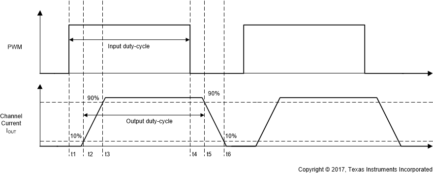
t(PWM_delay_rising) PWM rising edge delay, 50% PWM voltage to 10% of output current, t2 – t1 as shown in Figure 1 17 µs
t(PWM_delay_falling) PWM falling edge delay, 50% PWM voltage to 90% of output current, t5 – t4 as shown in Figure 1 21 µs
t(TSD_deg) Thermal overtemperature deglitch timer 60 µs
t(DEVICE_STARTUP) EN rising edge to 10% output current at 150-mA set current and 12-V supply voltage 100 150 µs
t(OPEN_deg) LED open-circuit fault-deglitch time 80 125 175 µs
t(SG_deg) Channel-output short-to-ground detection deglitch time 80 125 175 µs
t(Recover_deg) Recovery deglitch time 16 µs
TPS92611-Q1 PWM-dimming-measurment-SLDS233.gifFigure 1. Output Timing Diagram