SNVS902A October 2012 – October 2015 TPS92640 , TPS92641
PRODUCTION DATA.
- 1 Features
- 2 Applications
- 3 Description
- 4 Revision History
- 5 Pin Configuration and Functions
- 6 Specifications
-
7 Detailed Description
- 7.1 Overview
- 7.2 Functional Block Diagram
- 7.3
Feature Description
- 7.3.1 Controlled On-Time Architecture
- 7.3.2 Switching Frequency
- 7.3.3 Average LED Current
- 7.3.4 Analog Dimming and True-Zero Operation
- 7.3.5 Undervoltage Lockout (UVLO)
- 7.3.6 PWM Dimming Using the UDIM Pin
- 7.3.7 External Shunt FET PWM Dimming
- 7.3.8 VCC Regulation and Start-up
- 7.3.9 Precision Reference
- 7.3.10 Control Loop Compensation
- 7.3.11 Overcurrent Protection
- 7.3.12 Overvoltage Protection (OVP)
- 7.3.13 Boot Undervoltage Lockout (UVLO)
- 7.4 Device Functional Modes
-
8 Application and Implementation
- 8.1 Application Information
- 8.2
Typical Applications
- 8.2.1
TPS92640: Design Procedure
- 8.2.1.1 Design Requirements
- 8.2.1.2
Detailed Design Procedure
- 8.2.1.2.1 Set Output Voltage Feedback Ratio
- 8.2.1.2.2 Set Switching Frequency
- 8.2.1.2.3 Set Average LED Current
- 8.2.1.2.4 Set Inductor Ripple Current
- 8.2.1.2.5 Set LED Ripple Current and Determine Output Capacitance, COUT
- 8.2.1.2.6 Choose N-Channel MOSFETs
- 8.2.1.2.7 Choose Input Capacitance
- 8.2.1.2.8 Set the Turnon Voltage and Undervoltage Lockout Hysteresis
- 8.2.2
TPS92640 - PWM Dimming Application
- 8.2.2.1 Design Requirements
- 8.2.2.2
Detailed Design Procedure
- 8.2.2.2.1 Calculate Operating Points
- 8.2.2.2.2 Output Voltage Feedback
- 8.2.2.2.3 Switching Frequency
- 8.2.2.2.4 Set the Feedback Reference and LED Current
- 8.2.2.2.5 Calculate the Inductor Value
- 8.2.2.2.6 Calculate the Output Capacitor Value
- 8.2.2.2.7 Calculate the MOSFET Parameters
- 8.2.2.2.8 Calculate the Minimum Input Capacitance
- 8.2.2.2.9 Undervoltage Lockout and Hysteresis
- 8.2.2.3 Application Curve
- 8.2.1
TPS92640: Design Procedure
- 9 Power Supply Recommendations
- 10Layout
- 11Device and Documentation Support
- 12Mechanical, Packaging, and Orderable Information
Package Options
Mechanical Data (Package|Pins)
- PWP|14
Thermal pad, mechanical data (Package|Pins)
- PWP|14
Orderable Information
1 Features
- VIN Range from 7 V to 85 V
- Wide Dimming Range
- 500:1 Analog Dimming
- 2500:1 Standard PWM Dimming
- 20000:1 Shunt FET PWM Dimming
- Adjustable LED Current Sense Voltage
- 2-Ω, 1-Apeak MOSFET Gate Drivers
- Shunt Dimming MOSFET Gate Driver (TPS92641)
- Programmable Switching Frequency
- Precision Voltage Reference 3 V ±2%
- Input UVLO and Output OVP
- Low Power Shutdown Mode and Thermal Shutdown
2 Applications
- LED Driver / Constant Current Regulator
- Architectural LED Lighting Drivers
- Automotive LED Drivers
- General LED Illumination
3 Description
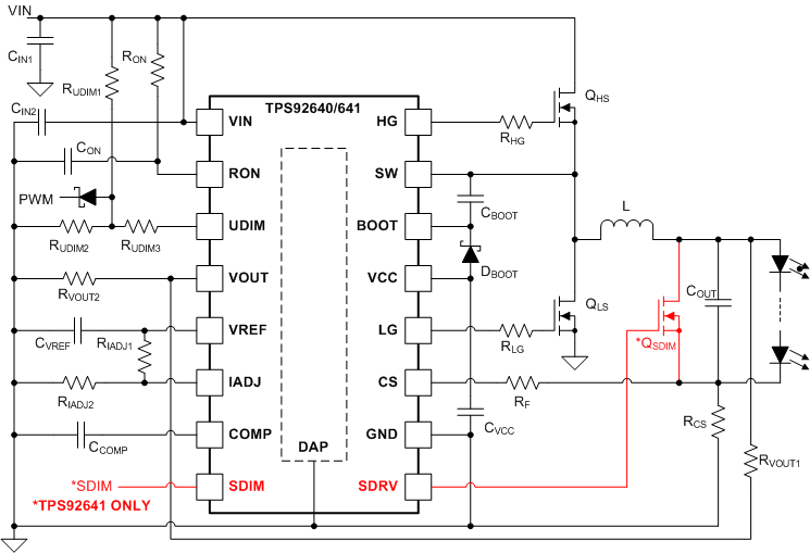
The TPS92640 and TPS92641 devices are high-voltage, synchronous NFET controllers for buck-current regulators. Output current regulation is based on valley current-mode operation using a controlled on-time architecture. This control method eases the design of loop compensation while maintaining nearly constant switching frequency. The TPS92640 and TPS92641 devices include a high-voltage start-up regulator that operates over a wide input range of 7 V to 85 V. The PWM controller is designed for high speed capability, including an oscillator frequency range up to 1 MHz. The deadtime between high side and low side gate driver is optimized to provide very high efficiency over a wide input operating voltage and output power range. The TPS92640 and TPS92641 devices accept both analog and PWM input signals, resulting in exceptional dimming control range. Linear response characteristics between input command and LED current is achieved with true zero LED current using low off-set error amplifier and proprietary PWM dimming logic. Both devices also include precision reference capable of supplying current to low power microcontroller. Protection features include cycle-by-cycle current protection, overvoltage protection, and thermal shutdown. The TPS92641 device includes a shunt FET dimming input and MOSFET driver for high resolution PWM dimming.
Device Information(1)
| PART NUMBER | PACKAGE | BODY SIZE (NOM) |
|---|---|---|
| TPS92640 | HTSSOP (14) | 4.40 mm × 5.00 mm |
| TPS92641 | HTSSOP (16) | 4.40 mm × 5.00 mm |
- For all available packages, see the orderable addendum at the end of the data sheet.
Typical Application Diagram
