SLVSD68 December 2015 TPS92691 , TPS92691-Q1
PRODUCTION DATA.
- 1 Features
- 2 Applications
- 3 Description
- 4 Revision History
- 5 Pin Configuration and Functions
- 6 Specifications
-
7 Detailed Description
- 7.1 Overview
- 7.2 Functional Block Diagram
- 7.3
Feature Description
- 7.3.1 Internal Regulator and Undervoltage Lockout (UVLO)
- 7.3.2 Oscillator
- 7.3.3 Gate Driver
- 7.3.4 Rail-to-Rail Current Sense Amplifier
- 7.3.5 Transconductance Error Amplifier
- 7.3.6 Switch Current Sense and Internal Slope Compensation
- 7.3.7 Analog Adjust Input
- 7.3.8 PWM Input and Series Dimming FET Gate Driver Output
- 7.3.9 Soft-Start
- 7.3.10 Current Monitor Output
- 7.3.11 Overvoltage Protection
- 7.3.12 Thermal Protection
- 7.4 Device Functional Modes
-
8 Application and Implementation
- 8.1
Application Information
- 8.1.1 Duty Cycle Considerations
- 8.1.2 Inductor Selection
- 8.1.3 Output Capacitor Selection
- 8.1.4 Input Capacitor Selection
- 8.1.5 Main Power MOSFET Selection
- 8.1.6 Rectifier Diode Selection
- 8.1.7 LED Current Programming
- 8.1.8 Switch Current Sense Resistor and Slope Compensation
- 8.1.9 Feedback Compensation
- 8.1.10 Soft-Start
- 8.1.11 Overvoltage Protection
- 8.1.12 PWM Dimming Considerations
- 8.2
Typical Applications
- 8.2.1
Typical Boost LED Driver
- 8.2.1.1 Design Requirements
- 8.2.1.2
Detailed Design Procedure
- 8.2.1.2.1 Calculating Duty Cycle
- 8.2.1.2.2 Setting Switching Frequency
- 8.2.1.2.3 Inductor Selection
- 8.2.1.2.4 Output Capacitor Selection
- 8.2.1.2.5 Input Capacitor Selection
- 8.2.1.2.6 Main N-Channel MOSFET Selection
- 8.2.1.2.7 Rectifying Diode Selection
- 8.2.1.2.8 Programming LED Current
- 8.2.1.2.9 Setting Switch Current Limit and Slope Compensation
- 8.2.1.2.10 Deriving Compensator Parameters
- 8.2.1.2.11 Setting Start-up Duration
- 8.2.1.2.12 Setting Overvoltage Protection Threshold
- 8.2.1.2.13 PWM Dimming Considerations
- 8.2.1.3 Application Curves
- 8.2.2
Typical Buck-Boost LED Driver
- 8.2.2.1 Design Requirements
- 8.2.2.2
Detailed Design Procedure
- 8.2.2.2.1 Calculating Duty Cycle
- 8.2.2.2.2 Setting Switching Frequency
- 8.2.2.2.3 Inductor Selection
- 8.2.2.2.4 Output Capacitor Selection
- 8.2.2.2.5 Input Capacitor Selection
- 8.2.2.2.6 Main N-Channel MOSFET Selection
- 8.2.2.2.7 Rectifier Diode Selection
- 8.2.2.2.8 Setting Switch Current Limit and Slope Compensation
- 8.2.2.2.9 Programming LED Current
- 8.2.2.2.10 Deriving Compensator Parameters
- 8.2.2.2.11 Setting Startup Duration
- 8.2.2.2.12 Setting Overvoltage Protection Threshold
- 8.2.2.2.13 PWM Dimming Consideration
- 8.2.2.3 Application Curves
- 8.2.1
Typical Boost LED Driver
- 8.1
Application Information
- 9 Power Supply Recommendations
- 10Layout
- 11Device and Documentation Support
- 12Mechanical, Packaging, and Orderable Information
Package Options
Mechanical Data (Package|Pins)
- PWP|16
Thermal pad, mechanical data (Package|Pins)
- PWP|16
Orderable Information
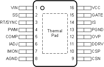
5 Pin Configuration and Functions
PWP Package
16-Pin HTSSOP with PowerPAD™
Top View

Pin Functions
| PIN | I/O | DESCRIPTION | |
|---|---|---|---|
| NO. | NAME | ||
| 1 | VIN | — | Input supply for the internal VCC regulator. Bypass with 100-nF capacitor to GND located close to the controller. |
| 2 | SS | I/O | Soft-start programming pin. Connect a capacitor to AGND to extend the start-up time. Switching can be disabled by shorting the pin to GND. |
| 3 | RT/SYNC | I/O | Oscillator frequency programming pin. Connect a resistor to AGND to set the switching frequency. The internal oscillator can be synchronized by coupling an external clock pulse through 100-nF series capacitor. |
| 4 | PWM | I | PWM dimming input. Driving the pin below 2.3 V (typ), turns off switching, idles the oscillator, disconnects the COMP pin, and sets DDRV output to ground. The input signal duty cycle controls the average LED current through PWM dimming operation. Connect to VCC when not used for PWM dimming. |
| 5 | COMP | I/O | Transconductance error amplifier output. Connect compensation network to achieve desired closed-loop response. |
| 6 | IADJ | I | LED current reference input. Connecting pin to VCC with 100-kΩ series resistor sets internal reference voltage to 2.42 V and the current sense threshold, V(CSP-CSN)to 172 mV. The pin can be modulated by external voltage source from 0 V to 2.25 V to implement analog dimming. |
| 7 | IMON | O | LED current report pin. The LED current sensed by CSP/CSN input is reported as VIMON = 14 × ILED × Rcs. Bypass with a 1-nF ceramic capacitor to AGND. |
| 8 | AGND | — | Analog ground. Return for the internal voltage reference and analog circuit. Connect to circuit ground, GND, to complete return path. |
| 9 | CSN | I | Current sense amplifier negative input (–). Connect directly to the negative node of LED current sense resistor RCS). |
| 10 | CSP | I | Current sense amplifier positive input (+). Connect directly to the positive node of LED current sense resistor RCS). |
| 11 | DDRV | O | Series dimming FET gate driver output. Connect to gate of external N-channel MOSFET or a level-shift circuit with P-channel MOSFET to implement series FET PWM dimming. |
| 12 | OVP | I | Hysteretic overvoltage protection input. Connect resistor divider from output voltage to set OVP threshold and hysteresis. |
| 13 | PGND | — | Power ground connection pin for internal N-channel MOSFET gate drivers. Connect to circuit ground, GND, to complete return path. |
| 14 | IS | I | Switch current sense input. Connected to the switch current sense resistor, RIS, in the source of the N-channel MOSFET. |
| 15 | GATE | O | N-channel MOSFET gate driver output. Connect to gate of external switching N-channel MOSFET. |
| 16 | VCC | — | VCC bias supply pin. Locally decouple to PGND using a 2.2-µF to 4.7-µF ceramic capacitor located close to the controller. |
| PowerPAD | — | The AGND and PGND pin must be connected to the exposed PowerPAD for proper operation. This PowerPAD must be connected to PCB ground plane using multiple vias for good thermal performance. | |