SLVSD68 December 2015 TPS92691 , TPS92691-Q1
PRODUCTION DATA.
- 1 Features
- 2 Applications
- 3 Description
- 4 Revision History
- 5 Pin Configuration and Functions
- 6 Specifications
-
7 Detailed Description
- 7.1 Overview
- 7.2 Functional Block Diagram
- 7.3
Feature Description
- 7.3.1 Internal Regulator and Undervoltage Lockout (UVLO)
- 7.3.2 Oscillator
- 7.3.3 Gate Driver
- 7.3.4 Rail-to-Rail Current Sense Amplifier
- 7.3.5 Transconductance Error Amplifier
- 7.3.6 Switch Current Sense and Internal Slope Compensation
- 7.3.7 Analog Adjust Input
- 7.3.8 PWM Input and Series Dimming FET Gate Driver Output
- 7.3.9 Soft-Start
- 7.3.10 Current Monitor Output
- 7.3.11 Overvoltage Protection
- 7.3.12 Thermal Protection
- 7.4 Device Functional Modes
-
8 Application and Implementation
- 8.1
Application Information
- 8.1.1 Duty Cycle Considerations
- 8.1.2 Inductor Selection
- 8.1.3 Output Capacitor Selection
- 8.1.4 Input Capacitor Selection
- 8.1.5 Main Power MOSFET Selection
- 8.1.6 Rectifier Diode Selection
- 8.1.7 LED Current Programming
- 8.1.8 Switch Current Sense Resistor and Slope Compensation
- 8.1.9 Feedback Compensation
- 8.1.10 Soft-Start
- 8.1.11 Overvoltage Protection
- 8.1.12 PWM Dimming Considerations
- 8.2
Typical Applications
- 8.2.1
Typical Boost LED Driver
- 8.2.1.1 Design Requirements
- 8.2.1.2
Detailed Design Procedure
- 8.2.1.2.1 Calculating Duty Cycle
- 8.2.1.2.2 Setting Switching Frequency
- 8.2.1.2.3 Inductor Selection
- 8.2.1.2.4 Output Capacitor Selection
- 8.2.1.2.5 Input Capacitor Selection
- 8.2.1.2.6 Main N-Channel MOSFET Selection
- 8.2.1.2.7 Rectifying Diode Selection
- 8.2.1.2.8 Programming LED Current
- 8.2.1.2.9 Setting Switch Current Limit and Slope Compensation
- 8.2.1.2.10 Deriving Compensator Parameters
- 8.2.1.2.11 Setting Start-up Duration
- 8.2.1.2.12 Setting Overvoltage Protection Threshold
- 8.2.1.2.13 PWM Dimming Considerations
- 8.2.1.3 Application Curves
- 8.2.2
Typical Buck-Boost LED Driver
- 8.2.2.1 Design Requirements
- 8.2.2.2
Detailed Design Procedure
- 8.2.2.2.1 Calculating Duty Cycle
- 8.2.2.2.2 Setting Switching Frequency
- 8.2.2.2.3 Inductor Selection
- 8.2.2.2.4 Output Capacitor Selection
- 8.2.2.2.5 Input Capacitor Selection
- 8.2.2.2.6 Main N-Channel MOSFET Selection
- 8.2.2.2.7 Rectifier Diode Selection
- 8.2.2.2.8 Setting Switch Current Limit and Slope Compensation
- 8.2.2.2.9 Programming LED Current
- 8.2.2.2.10 Deriving Compensator Parameters
- 8.2.2.2.11 Setting Startup Duration
- 8.2.2.2.12 Setting Overvoltage Protection Threshold
- 8.2.2.2.13 PWM Dimming Consideration
- 8.2.2.3 Application Curves
- 8.2.1
Typical Boost LED Driver
- 8.1
Application Information
- 9 Power Supply Recommendations
- 10Layout
- 11Device and Documentation Support
- 12Mechanical, Packaging, and Orderable Information
Package Options
Mechanical Data (Package|Pins)
- PWP|16
Thermal pad, mechanical data (Package|Pins)
- PWP|16
Orderable Information
10 Layout
10.1 Layout Guidelines
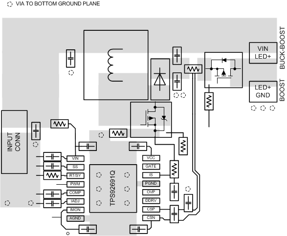
- The performance of the switching regulator depends as much on the layout of the PCB as the component selection. Following a few simple guidelines will maximize noise rejection and minimize the generation of EMI within the circuit.
- Discontinuous currents are the most likely to generate EMI. Therefore, take care when routing these paths. The main path for discontinuous current in the TPS92691/-Q1 Buck regulator contains the input capacitor, CIN, the recirculating diode, D, the N-channel MOSFET, Q1, and the sense resistor, RIS. In the TPS92691/-Q1 Boost regulator, the discontinuous current flows through the output capacitor COUT, diode, D, N-channel MOSFET, Q1, and the current sense resistor, RIS. In Buck-Boost regulator, both loops are discontinuous and should be carefully laid out. These loops should be kept as small as possible and the connection between all the components should be short and thick to minimize parasitic inductance. In particular, the switch node (where L, D, and Q1 connect) should be just large enough to connect the components. To minimize excessive heating, large copper pours can be placed adjacent to the short current path of the switch node.
- CSP and CSN traces should be routed together with Kelvin connections to the current sense resistor as short as possible. If needed, use common mode and differential mode noise filters to attenuate switching and diode reverse recovery noise from affecting the internal current sense amplifier.
- The COMP, IS, OVP, PWM, and IADJ pins are all high-impedance inputs that couple external noise easily; therefore, the loops containing these nodes should be minimized whenever possible.
- In some applications, the LED or LED array can be far away from the TPS92691/-Q1, or on a separate PCB connected by a wiring harness. When an output capacitor is used and the LED array is large or separated from the rest of the regulator, the output capacitor should be placed close to the LEDs to reduce the effects of parasitic inductance on the AC impedance of the capacitor.
- The TPS92691/-Q1 has an exposed thermal pad to aid power dissipation. Adding several vias under the exposed pad helps conduct heat away from the device. The junction-to-ambient thermal resistance varies with application. The most significant variables are the area of copper in the PCB and the number of vias under the exposed pad. The integrity of the solder connection from the device exposed pad to the PCB is critical. Excessive voids greatly decrease the thermal dissipation capacity.
10.2 Layout Example
 Figure 45. Layout Recommendation