SLVSG64B February 2022 – November 2022 TPSM82903
PRODUCTION DATA
- 1 Features
- 2 Applications
- 3 Description
- 4 Revision History
- 5 Pin Configuration and Functions
- 6 Specifications
-
7 Detailed Description
- 7.1 Overview
- 7.2 Functional Block Diagram
- 7.3
Feature Description
- 7.3.1 Mode Selection and Device Configuration (MODE/S-CONF)
- 7.3.2 Adjustable VO Operation (External Voltage Divider)
- 7.3.3 Setable VO Operation (VSET and Internal Voltage Divider)
- 7.3.4 Soft Start/Tracking (SS/TR)
- 7.3.5 Smart Enable with Precise Threshold
- 7.3.6 Power Good (PG)
- 7.3.7 Undervoltage Lockout (UVLO)
- 7.3.8 Current Limit And Short Circuit Protection
- 7.3.9 Thermal Shutdown
- 7.4 Device Functional Modes
- 8 Application and Implementation
- 9 Device and Documentation Support
- 10Mechanical, Packaging, and Orderable Information
Package Options
Mechanical Data (Package|Pins)
- SIS|11
Thermal pad, mechanical data (Package|Pins)
Orderable Information
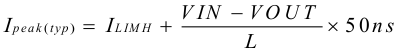
7.3.8 Current Limit And Short Circuit Protection
The TPSM82903 is protected against overload and short circuit events. If the inductor current exceeds the high-side FET current limit (ILIMH), the high-side switch is turned off and the low-side switch is turned on to ramp down the inductor current. The high-side FET turns on again only if the current in the low-side FET has decreased below the low-side FET current limit threshold.
Due to internal propagation delay, the actual current can exceed the static current limit during that time. The dynamic current limit is given as Equation 1:
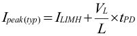
where
- ILIMH is the static high-side FET current limit as specified in the Electrical Characteristics.
- L is the effective inductance at the peak current (approximately 0.9 μH).
- VL is the voltage across the inductor (VIN – VOUT).
- tPD is the internal propagation delay of typically 50 ns.
The current limit can exceed static values, especially if the input voltage is high and very small inductances are used. The dynamic high-side switch peak current can be calculated as follows: