SLVSGJ4C october 2022 – july 2023 TPSM82912 , TPSM82913 , TPSM82913E
PRODUCTION DATA
- 1
- 1 Features
- 2 Applications
- 3 Description
- 4 Revision History
- 5 Pin Configuration and Functions
- 6 Specifications
-
7 Detailed Description
- 7.1 Overview
- 7.2 Functional Block Diagram
- 7.3
Feature Description
- 7.3.1 Smart Config (S-CONF)
- 7.3.2 Device Enable (EN/SYNC)
- 7.3.3 Device Synchronization (EN/SYNC)
- 7.3.4 Spread Spectrum Modulation
- 7.3.5 Output Discharge
- 7.3.6 Undervoltage Lockout (UVLO)
- 7.3.7 Power-Good Output
- 7.3.8 Noise Reduction and Soft-Start Capacitor (NR/SS)
- 7.3.9 Current Limit and Short-Circuit Protection
- 7.3.10 Thermal Shutdown
- 7.4 Device Functional Modes
- 8 Application and Implementation
- 9 Device and Documentation Support
- 10Mechanical, Packaging, and Orderable Information
Package Options
Mechanical Data (Package|Pins)
- RDU|28
Thermal pad, mechanical data (Package|Pins)
Orderable Information
8.2 Typical Applications
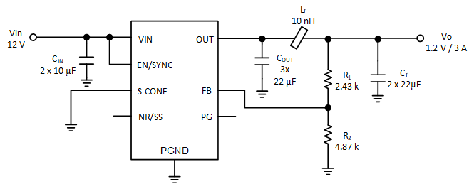
 Figure 8-1 Typical Schematic
Table 8-1 shows the list of components for the application curves in Section 8.2.3, unless otherwise noted.
Table 8-1 List of Components
| REFERENCE | PART NUMBER | DESCRIPTION | MANUFACTURER(1) |
|---|---|---|---|
| TPSM82913 | TPSM82913 | Low-noise and low-ripple buck module | Texas Instruments |
| CIN | C2012X7S1E106K125AC | Ceramic capacitors: 2 × 10 µF ±10% 25-V ceramic capacitor X7S 0805 | TDK |
| COUT | C2012X7S1A226M125AC | Ceramic capacitors: 3 × 22 µF, 10 V, ±20%, X7S, 0805 | TDK |
| Lf | BLE18PS080SN1 | Ferrite Bead | MuRata |
| Cf | C2012X7S1A226M125AC | Ceramic capacitor: 2 × 22 µF, 10 V, ±20%, X7S, 0805 | TDK |
| CNR/SS, CFF | Optional, not shown | Ceramic capacitor | Standard |
| R1, R2 | Resistor | Standard |
(1) See the Third-Party Products Disclaimer