SLASE39 May 2014 TRF37A73
PRODUCTION DATA.
- 1 Features
- 2 Applications
- 3 Description
- 4 Revision History
- 5 Pin Configuration and Functions
- 6 Specifications
- 7 Detailed Description
- 8 Applications and Implementation
- 9 Power Supply Recommendations
- 10Layout
- 11Device and Documentation Support
- 12Mechanical, Packaging, and Orderable Information
Package Options
Mechanical Data (Package|Pins)
- DSG|8
Thermal pad, mechanical data (Package|Pins)
- DSG|8
Orderable Information
10 Layout
10.1 Layout Guidelines
Good layout practice helps to enable excellent linearity and isolation performance. An example of good layout is shown in Figure 15. In the example, only the top signal layer and its adjacent ground reference plane are shown.
- Excellent electrical connection from the PowerPAD™ to the board ground is essential. Use the recommended footprint, solder the pad to the board, and do not include solder mask under the pad.
- Connect pad ground to device terminal ground on the top board layer.
- Verify that the return DC and RF current path have a low impedance ground plane directly under the package and RF signal traces into and out of the amplifier.
- Ensure that ground planes on the top and any internal layers are well stitched with vias.
- Do not route RF signal lines over breaks in the reference ground plane.
- Avoid routing clocks and digital control lines near RF signal lines.
- Do not route RF or DC signal lines over noisy power planes. Ground is the best reference, although clean power planes can serve where necessary.
- Place supply decoupling close to the device.
10.2 Layout Example
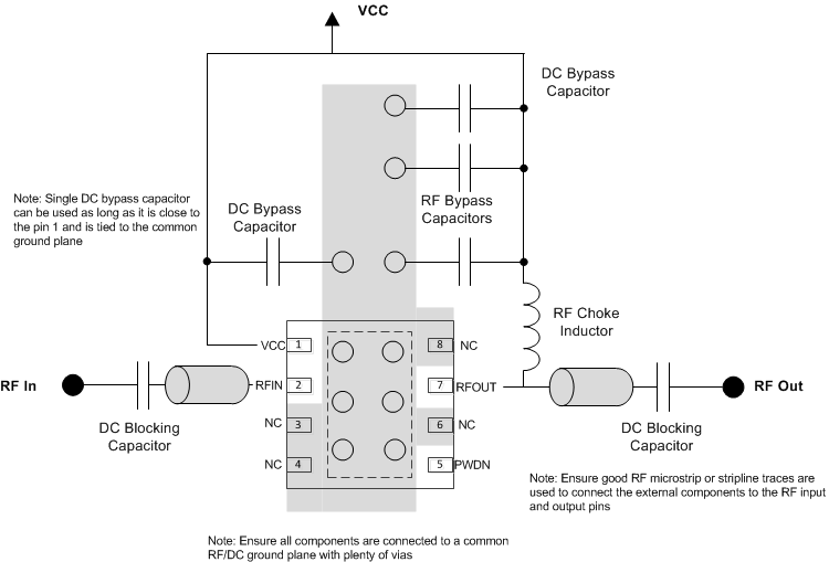 Figure 15. Layout