SLASE37A May 2014 – December 2014 TRF37A32 , TRF37B32 , TRF37C32
PRODUCTION DATA.
- 1 Features
- 2 Applications
- 3 Description
- 4 Simplified Schematic
- 5 Revision History
- 6 Pin Configuration and Functions
-
7 Specifications
- 7.1 Absolute Maximum Ratings
- 7.2 ESD Ratings
- 7.3 Recommended Operating Conditions
- 7.4 Thermal Information
- 7.5 Electrical Characteristics, TRF37A32
- 7.6 Electrical Characteristics, TRF37B32
- 7.7 Electrical Characteristics, TRF37C32
- 7.8 Timing Requirements
- 7.9 Typical Characteristics (TRF37A32)
- 7.10 Typical Characteristics (TRF37B32)
- 7.11 Typical Characteristics (TRF37C32)
- 8 Detailed Description
- 9 Applications and Implementation
- 10Power Supply Recommendations
- 11Layout
- 12Device and Documentation Support
Package Options
Mechanical Data (Package|Pins)
- RTV|32
Thermal pad, mechanical data (Package|Pins)
- RTV|32
Orderable Information
7 Specifications
7.1 Absolute Maximum Ratings
over operating free-air temperature range (unless otherwise noted) (1)| MIN | MAX | UNIT | ||
|---|---|---|---|---|
| Input voltage | –0.3 | 3.6 | V | |
| Storage temperature, TSTG | –40 | 150 | °C |
(1) Stresses beyond those listed under Absolute Maximum Ratings may cause permanent damage to the device. These are stress ratings only, which do not imply functional operation of the device at these or any other conditions beyond those indicated under Recommended Operating Conditions. Exposure to absolute-maximum-rated conditions for extended periods may affect device reliability.
7.2 ESD Ratings
| VALUE | UNIT | ||||
|---|---|---|---|---|---|
| V(ESD) | Electrostatic discharge | Human-body model (HBM), per ANSI/ESDA/JEDEC JS-001(1) | All pins except XIFOUTAP, IFOUTAN, IFOUTBP, and IFOUTBN | ±2500 | V |
| Pins XIFOUTAP, IFOUTAN, IFOUTBP, and IFOUTBN (2) | ±100 | ||||
| Charged-device model (CDM), per JEDEC specification JESD22-C101(3) | ±1000 | ||||
(1) JEDEC document JEP155 states that 500-V HBM allows safe manufacturing with a standard ESD control process.
(2) High Linearity IFOUT pins are susceptible to low voltage HBM damage.
(3) JEDEC document JEP157 states that 250-V CDM allows safe manufacturing with a standard ESD control process.
7.3 Recommended Operating Conditions
over operating free-air temperature range (unless otherwise noted)| MIN | NOM | MAX | UNIT | ||
|---|---|---|---|---|---|
| Operating virtual junction temperature range, TJ | –40 | 125 | °C | ||
7.4 Thermal Information
| THERMAL METRIC(1) | RTV | UNIT | |
|---|---|---|---|
| 32 PINS | |||
| RθJA | Junction-to-ambient thermal resistance | 32.3 | °C/W |
| RθJCtop | Junction-to-case (top) thermal resistance | 19.8 | |
| RθJB | Junction-to-board thermal resistance | 5.9 | |
| ψJT | Junction-to-top characterization parameter | 0.2 | |
| ψJB | Junction-to-board characterization parameter | 5.9 | |
| RθJCbot | Junction-to-case (bottom) thermal resistance | 1.3 | |
(1) For more information about traditional and new thermal metrics, see the IC Package Thermal Metrics application report, SPRA953.
7.5 Electrical Characteristics, TRF37A32
TA = 25°C, VCC = 3.3 V; PRF = –10 dBm; PLO = 0 dBm; FIF = 200 MHz; Low Side Injection, LPM = 0 (unless otherwise noted)| PARAMETER | TEST CONDITIONS | MIN | TYP | MAX | UNIT | |
|---|---|---|---|---|---|---|
| DC Parameters | ||||||
| VCC | Supply Voltage | 3.15 | 3.3 | 3.45 | V | |
| ICC | Supply Current | FLO = 750 MHz | 280 | mA | ||
| Pdiss | Total Power Dissipation | FLO = 750 MHz | 0.92 | W | ||
| Power Down Current | 2 | mA | ||||
| RF Frequency Range | ||||||
| FRF | Frequency Range | 400 | 1700 | MHz | ||
| RF Specifications | ||||||
| G | Gain | FRF = 950 MHz (LSI) | 9.6 | dB | ||
| Gvar | Gain Variation over Frequency | within any 200 MHz Band | 0.5 | dB | ||
| NF | SSB Noise Figure | FRF = 950 MHz (LSI) | 9.6 | dB | ||
| SSB Noise Figure with Blocker | 5 dBm blocker signal Δf > 50 MHz |
17 | dB | |||
| IIP3 | Input 3rd Order Intercept Point | FRF = 950 MHz (LSI), Fspacing = 20 MHz |
26 | dBm | ||
| OIP3 | Output 3rd Order Intercept Point | FRF = 950 MHz (LSI), Fspacing = 20 MHz |
35.6 | dBm | ||
| OIP2 | Output 2nd Order Intercept Point | FRF = 950 MHz (LSI) | 65 | dBm | ||
| IP1dB | Input 1 dB Compression Point | FRF = 950 MHz (LSI) | 11 | dBm | ||
| ZIN | Input Impedance | 50 | Ω | |||
| RLi | Input Return Loss | FRF = 800 - 1400 MHz (LSI) | 15 | dB | ||
| LO Input | ||||||
| PLO | LO Drive Level | –3 | 0 | 6 | dBm | |
| FLO | LO Frequency Range | 600 | 1400 | MHz | ||
| ZIN | Input Impedance | 50 | Ω | |||
| RLi | Input Return Loss | FRF = 750 - 1150 MHz | 15 | dB | ||
| Low Power Mode: LPM = 1 | ||||||
| ICC | Supply Current | FLO = 750 MHz | 200 | mA | ||
| Pdiss | Total Power Dissipation | FLO = 750 MHz | 0.66 | W | ||
| G | Gain | FRF = 950 MHz (LSI) | 9.2 | dB | ||
| NF | SSB Noise Figure | FRF = 950 MHz (LSI) | 9.6 | dB | ||
| IIP3 | Input 3rd Order Intercept Point | FRF = 950 MHz (LSI), Fspacing = 20 MHz |
26 | dBm | ||
| IP1dB | Input 1 dB Compression Point | FRF = 950 MHz (LSI) | 11 | dBm | ||
| Isolation | ||||||
| Channel Isolation | Drive RFinA/B IFoutA/B-IFoutB/A FRF = 950 MHz |
50 | dB | |||
| RF to IF Isolation | FRF = 950 MHz | 20 | dB | |||
| LO to RF Leakage | PLO = 0 dBm | –55 | dBm | |||
| LO to IF Leakage | PLO = 0 dBm | –45 | dBm | |||
| Spurious | ||||||
| 2x2 Spurious Product | 2RF - 2LO | 65 | dBc | |||
| 3x3 Spurious Product | 3RF - 3LO | 70 | dBc | |||
| IF Output | ||||||
| ZL | Differential Output Impedance Load | 200 | Ω | |||
| FIF | Frequency Range | 1 dB corner frequency | 30 | 600 | MHz | |
| DC Bias Range | Externally supplied DC bias through RF choke | 3.3 | V | |||
7.6 Electrical Characteristics, TRF37B32
TA = 25°C, VCC = 3.3 V; PRF = –10 dBm; PLO = 0 dBm; FIF = 200 MHz; Low Side Injection, LPM = 0 (unless otherwise noted)| PARAMETER | TEST CONDITIONS | MIN | TYP | MAX | UNIT | |
|---|---|---|---|---|---|---|
| DC Parameters | ||||||
| VCC | Supply Voltage | 3.15 | 3.3 | 3.45 | V | |
| ICC | Supply Current | FLO = 1750 MHz | 305 | mA | ||
| Pdiss | Total Power Dissipation | FLO = 1750 MHz | 1 | W | ||
| Power Down Current | 2 | mA | ||||
| RF Frequency Range | ||||||
| FRF | Frequency Range | 700 | 2700 | MHz | ||
| RF Specifications | ||||||
| G | Gain | FRF = 1950 MHz (LSI) | 10 | dB | ||
| Gvar | Gain Variation over Frequency | within any 200 MHz Band | 0.5 | dB | ||
| NF | SSB Noise Figure | FRF = 1950 MHz (LSI) | 9.2 | dB | ||
| SSB Noise Figure with Blocker | 5 dBm blocker signal Δf > 50 MHz |
15.5 | dB | |||
| IIP3 | Input 3rd Order Intercept Point | FRF = 1950 MHz (LSI), Fspacing = 20 MHz |
32 | dBm | ||
| OIP3 | Output 3rd Order Intercept Point | FRF = 1950 MHz (LSI), Fspacing = 20 MHz |
42 | dBm | ||
| OIP2 | Output 2nd Order Intercept Point | FRF = 1950 MHz (LSI) | 70 | dBm | ||
| IP1dB | Input 1 dB Compression Point | FRF = 1950 MHz (LSI) | 10.8 | dBm | ||
| ZIN | Input Impedance | 50 | Ω | |||
| RLi | Input Return Loss | FRF = 1700 - 2700 MHz (LSI) | 10 | dB | ||
| LO Input | ||||||
| PLO | LO Drive Level | –3 | 0 | 6 | dBm | |
| FLO | LO Frequency Range | 500 | 2900 | MHz | ||
| ZIN | Input Impedance | 50 | Ω | |||
| RLi | Input Return Loss | FRF = 1500 - 2450 MHz | 15 | dB | ||
| Low Power Mode: LPM = 1 | ||||||
| ICC | Supply Current | FLO = 1750 MHz | 220 | mA | ||
| Pdiss | Total Power Dissipation | FLO = 1750 MHz | 0.73 | W | ||
| G | Gain | FRF = 1950 MHz (LSI) | 9.2 | dB | ||
| NF | SSB Noise Figure | FRF = 1950 MHz (LSI) | 9.2 | dB | ||
| IIP3 | Input 3rd Order Intercept Point | FRF = 1950 MHz (LSI), Fspacing = 20 MHz |
23 | dBm | ||
| IP1dB | Input 1 dB Compression Point | FRF = 1950 MHz (LSI) | 10.7 | dBm | ||
| Isolation | ||||||
| Channel Isolation | Drive RFinA/B IFoutA/B-IFoutB/A FRF = 1950 MHz |
45 | dB | |||
| RF to IF Isolation | FRF = 1950 MHz | 22 | dB | |||
| LO to RF Leakage | PLO = 0 dBm | –50 | dBm | |||
| LO to IF Leakage | PLO = 0 dBm | –42 | dBm | |||
| Spurious | ||||||
| 2x2 Spurious Product | 2RF - 2LO | 70 | dBc | |||
| 3x3 Spurious Product | 3RF - 3LO | 75 | dBc | |||
| IF Output | ||||||
| ZL | Differential Output Impedance Load | 200 | Ω | |||
| FIF | Frequency Range | 1 dB corner frequency | 30 | 600 | MHz | |
| DC Bias Range | Externally supplied DC bias through RF choke | 3.3 | V | |||
7.7 Electrical Characteristics, TRF37C32
TA = 25°C, VCC = 3.3 V; PRF = –10 dBm; PLO = 0 dBm; FIF = 200 MHz; Low Side Injection, LPM = 0 (unless otherwise noted)| PARAMETER | TEST CONDITIONS | MIN | TYP | MAX | UNIT | |
|---|---|---|---|---|---|---|
| DC Parameters | ||||||
| VCC | Supply Voltage | 3.15 | 3.3 | 3.45 | V | |
| ICC | Supply Current | FLO = 2300 MHz | 325 | mA | ||
| Pdiss | Total Power Dissipation | FLO = 2300 MHz | 1.1 | W | ||
| Power Down Current | 2 | mA | ||||
| RF Frequency Range | ||||||
| FRF | Frequency Range | 1700 | 3800 | MHz | ||
| RF Specifications | ||||||
| G | Gain | FRF = 2500 MHz (LSI) | 9.8 | dB | ||
| Gvar | Gain Variation over Frequency | within any 200 MHz Band | 0.5 | dB | ||
| NF | SSB Noise Figure | FRF = 2500 MHz (LSI) | 9.9 | dB | ||
| SSB Noise Figure with Blocker | 5 dBm blocker signal Δf > 50 MHz |
17.5 | dB | |||
| IIP3 | Input 3rd Order Intercept Point | FRF = 2500 MHz (LSI) Fspacing = 20 MHz |
29 | dBm | ||
| OIP3 | Output 3rd Order Intercept Point | FRF = 2500 MHz (LSI) Fspacing = 20 MHz |
38.8 | dBm | ||
| OIP2 | Output 2nd Order Intercept Point | FRF = 2500 MHz (LSI) | 65 | dBm | ||
| IP1dB | Input 1 dB Compression Point | FRF = 2500 MHz (LSI) | 11.5 | dBm | ||
| ZIN | Input Impedance | 50 | Ω | |||
| RLi | Input Return Loss | 8 | dB | |||
| LO Input | ||||||
| PLO | LO Drive Level | –3 | 0 | 6 | dBm | |
| FLO | LO Frequency Range | 1500 | 3600 | MHz | ||
| ZIN | Input Impedance | 50 | Ω | |||
| RLi | Input Return Loss | FRF = 2800 - 3400 MHz | 10 | dB | ||
| Low Power Mode: LPM = 1 | ||||||
| ICC | Supply Current | FLO = 2300 MHz | 230 | mA | ||
| Pdiss | Total Power Dissipation | FLO = 2300 MHz | 0.76 | W | ||
| G | Gain | FRF = 2500 MHz (LSI) | 9.2 | dB | ||
| NF | SSB Noise Figure | FRF = 2500 MHz (LSI) | 9.9 | dB | ||
| IIP3 | Input 3rd Order Intercept Point | FRF = 2500 MHz (LSI), Fspacing = 20 MHz |
22 | dBm | ||
| IP1dB | Input 1 dB Compression Point | FRF = 2500 MHz (LSI) | 11.5 | dBm | ||
| Isolation | ||||||
| Channel Isolation | Drive RFinA/B IFoutA/B-IFoutB/A FRF = 2500 MHz |
48 | dB | |||
| RF to IF Isolation | FRF = 2500 MHz | 21 | dB | |||
| LO to RF Leakage | PLO = 0 dBm | –55 | dBm | |||
| LO to IF Leakage | PLO = 0 dBm | –45 | dBm | |||
| Spurious | ||||||
| 2x2 Spurious Product | 2RF - 2LO | 65 | dBc | |||
| 3x3 Spurious Product | 3RF - 3LO | 70 | dBc | |||
| IF Output | ||||||
| ZL | Differential Output Impedance Load | 200 | Ω | |||
| FIF | Frequency Range | 1 dB corner frequency | 30 | 600 | MHz | |
| DC Bias Range | Externally supplied DC bias through RF choke | 3.3 | V | |||
7.8 Timing Requirements
| MIN | TYP | MAX | UNIT | |||
|---|---|---|---|---|---|---|
| Power Control | ||||||
| PD | Turn-on Time | PD = low to 90% final output power | 100 | ns | ||
| Turn-off Time | PD = high to initial output power –30 dB | 100 | ns | |||
7.9 Typical Characteristics (TRF37A32)
TA = 25°C, VCC = 3.3 V; PRF = –10 dBm; FRF = 950 MHz; PLO = 0 dBm; FIF = 200 MHz; Low Side Injection, LPM = 0 (unless otherwise noted)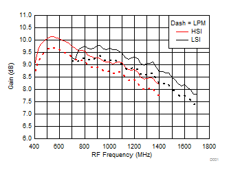

7.10 Typical Characteristics (TRF37B32)
TA = 25°C, VCC = 3.3 V; PRF = –10 dBm; FRF = 1950 MHz; PLO = 0 dBm; FIF = 200 MHz; Low Side Injection, LPM = 0 (unless otherwise noted)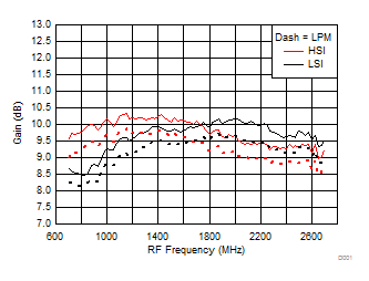
A.
Figure 25. Gain vs Frequency over H/LSI, LPM
A.
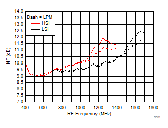
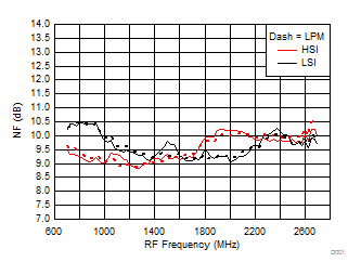
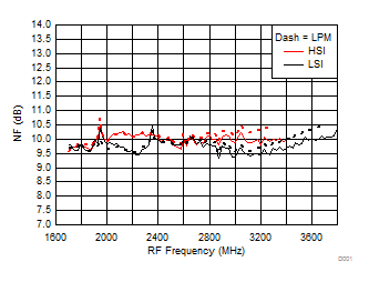
Figure 27. NF vs Frequency over H/LSI, LPM
A.
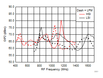
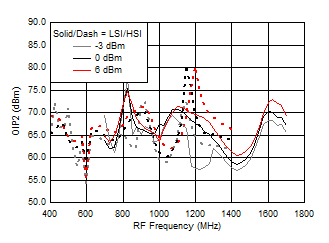
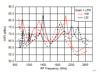
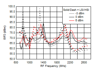
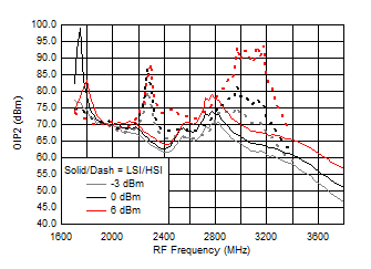
Figure 29. OIP2 vs Frequency over H/LSI, LPM
A.
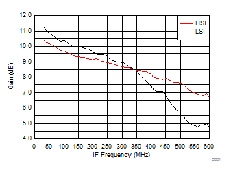
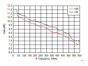
Figure 31. Gain vs IF Frequency over H/LSI
A.
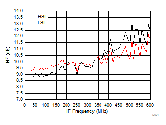
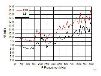
Figure 33. NF vs IF Frequency over H/LSI
A.
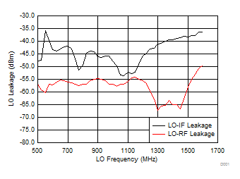
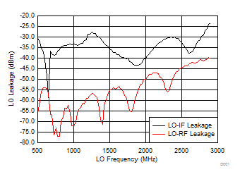
Figure 35. LO-IF/RF Leakage vs Frequency
A.
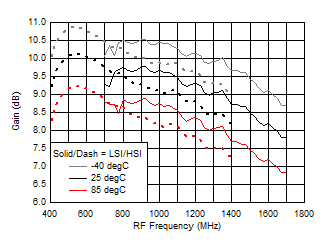
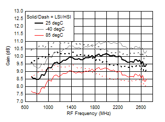
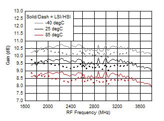
Figure 37. Gain vs Frequency over Temperature (HSI/LSI)
A.
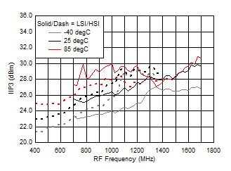
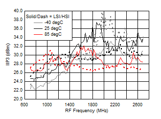
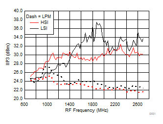
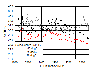
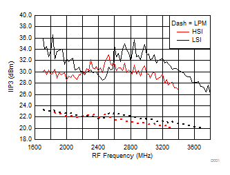
Figure 39. IIP3 vs Frequency over Temperature (HSI/LSI)
A.
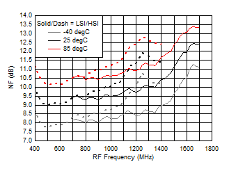
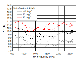
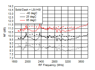
Figure 41. NF vs Frequency over Temperature (HSI/LSI)
A.
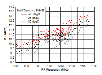
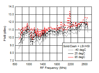
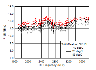
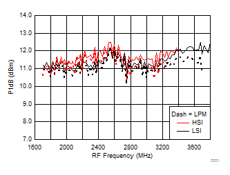
Figure 43. Input P1dB vs Frequency over Temperature (HSI/LSI)
A.
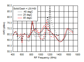
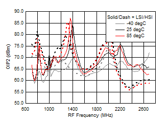
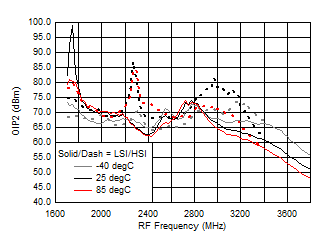
Figure 45. OIP2 vs Frequency over Temperature (HSI/LSI)
A.
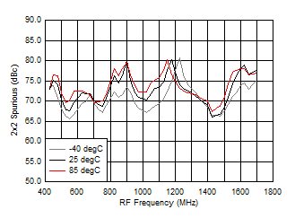
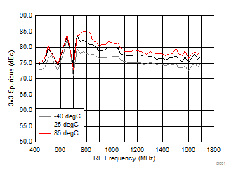
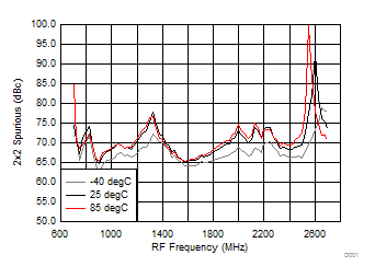
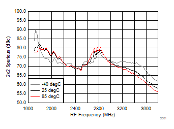
Figure 47. 2 x 2 Spurious over Temperature (H/LSI)
A.
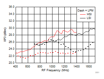
Figure 26. IIP3 vs Frequency over H/LSI, LPM
A.
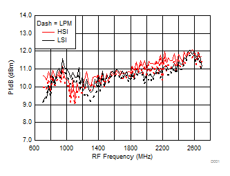
Figure 28. Input P1dB vs Frequency over H/LSI, LPM
A.
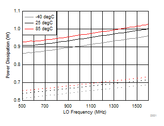
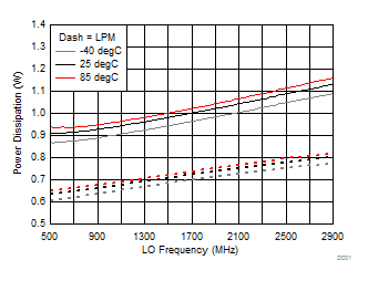
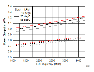
Figure 30. Power Dissipation vs Temperature, LPM
A.
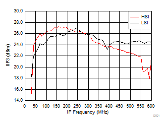
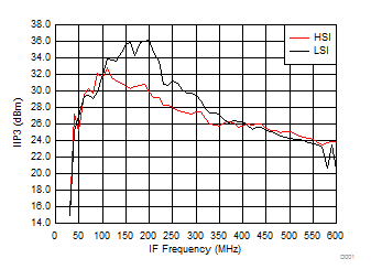
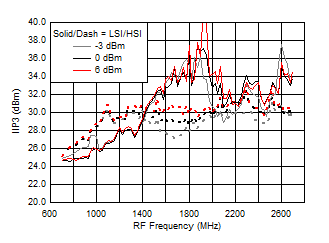
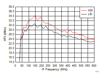
Figure 32. IIP3 vs IF Frequency over H/LSI
A.
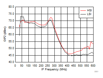
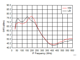
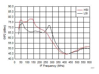
Figure 34. OIP2 vs IF Frequency over H/LSI
A.
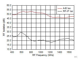
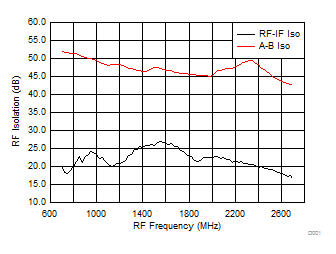
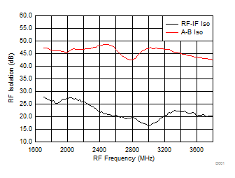
Figure 36. A-B Channel and RF-IF Isolation

A.
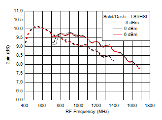
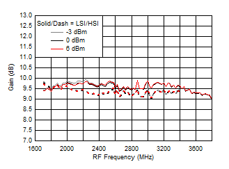
Figure 38. Gain vs Frequency over LO Drive (H/LSI)
A.
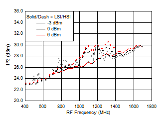
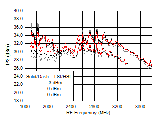
Figure 40. IIP3 vs Frequency over LO Drive (H/LSI)
A.
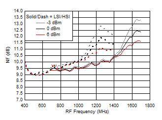
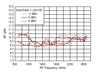
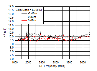
Figure 42. NF vs Frequency over LO Drive (H/LSI)
A.
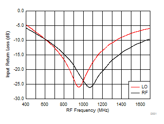
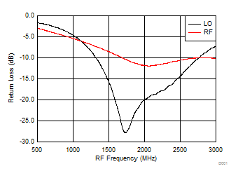
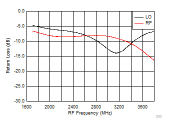
Figure 44. RF/LO Input Return Loss
A.
Figure 46. OIP2 vs Frequency over LO Drive (H/LSI)
A.
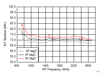
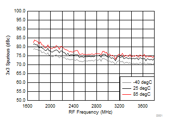
Figure 48. 3 x 3 Spurious over Temperature (H/LSI)
7.11 Typical Characteristics (TRF37C32)
TA = 25°C, VCC = 3.3 V; PRF = –10 dBm; FRF = 2500 MHz; PLO = 0 dBm; FIF = 200 MHz; Low Side Injection, LPM = 0 (unless otherwise noted)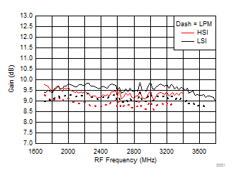
A.
Figure 49. Gain vs Frequency over H/LSI, LPM
A.
Figure 51. NF vs Frequency over H/LSI, LPM
A.
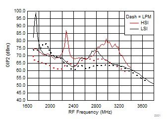
Figure 53. OIP2 vs Frequency over H/LSI, LPM
A.
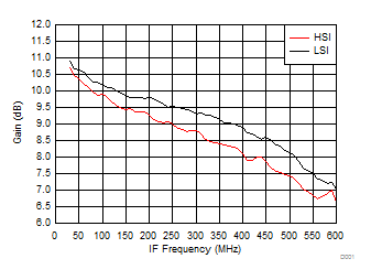
Figure 55. Gain vs IF Frequency over H/LSI
A.
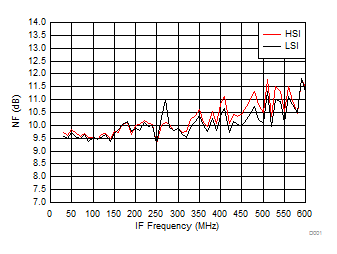
Figure 57. NF vs IF Frequency over H/LSI
A.
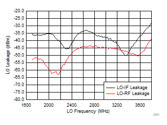
Figure 59. LO-IF/RF Leakage vs Frequency
A.
Figure 61. Gain vs Frequency over Temperature (HSI/LSI)
A.
Figure 63. IIP3 vs Frequency over Temperature (HSI/LSI)
A.
Figure 65. NF vs Frequency over Temperature (HSI/LSI)
A.
Figure 67. Input P1dB vs Frequency over Temperature (HSI/LSI)
A.
Figure 69. OIP2 vs Frequency over Temperature (HSI/LSI)
A.
Figure 71. 2 x 2 Spurious over Temperature (H/LSI)
A.
Figure 50. IIP3 vs Frequency over H/LSI, LPM
A.
Figure 52. Input P1dB vs Frequency over H/LSI, LPM
A.
Figure 54. Power Dissipation vs Temperature, LPM
A.
Figure 56. IIP3 vs IF Frequency over H/LSI
A.
Figure 58. OIP2 vs IF Frequency over H/LSI
A.
Figure 60. A-B Channel and RF-IF Isolation
A.
Figure 62. Gain vs Frequency over LO Drive (H/LSI)
A.
Figure 64. IIP3 vs Frequency over LO Drive (H/LSI)
A.
Figure 66. NF vs Frequency over LO Drive (H/LSI)
A.
Figure 68. RF/LO Input Return Loss
A.
Figure 70. OIP2 vs Frequency over LO Drive (H/LSI)
A.
Figure 72. 3 x 3 Spurious over Temperature (H/LSI)