SLOU186G August 2006 – May 2017 TRF7960 , TRF7961
PRODUCTION DATA.
- 1Device Overview
- 2Revision History
- 3Device Comparison
- 4Terminal Configuration and Functions
- 5Specifications
-
6Detailed Description
- 6.1 Overview
- 6.2 Power Supplies
- 6.3 Receiver - Analog Section
- 6.4 Register Descriptions
- 6.5
Direct Commands From MCU to Reader
- 6.5.1 Command Codes
- 6.5.2 Reset FIFO
- 6.5.3 Transmission With CRC
- 6.5.4 Transmission Without CRC
- 6.5.5 Delayed Transmission With CRC
- 6.5.6 Delayed Transmission Without CRC
- 6.5.7 Transmit Next Time Slot
- 6.5.8 Receiver Gain Adjust
- 6.5.9 Test External RF (RSSI at RX Input With TX Off)
- 6.5.10 Test Internal RF (RSSI at RX Input With TX On)
- 6.5.11 Block Receiver
- 6.5.12 Enable Receiver
- 6.6 Reader Communication Interface
- 6.7 Parallel Interface Communication
- 6.8 Serial Interface Communication
- 7Applications, Implementation, and Layout
- 8Device and Documentation Support
- 9Mechanical, Packaging, and Orderable Information
Package Options
Mechanical Data (Package|Pins)
- RHB|32
Thermal pad, mechanical data (Package|Pins)
- RHB|32
Orderable Information
4 Terminal Configuration and Functions
4.1 Pin Diagram
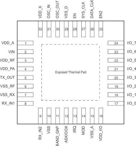
Figure 4-1 shows the pinout of the 32-pin RHB package.
 Figure 4-1 32-Pin RHB Package (Top View)
4.2 Signal Descriptions
Table 4-1 describes the device signals.
Table 4-1 Signal Descriptions
| TERMINAL | TYPE(1) | DESCRIPTION | |
|---|---|---|---|
| NAME | NO. | ||
| VDD_A | 1 | OUT | Internal regulated supply (2.7 V to 3.4 V) for analog circuitry |
| VIN | 2 | SUP | External supply input to chip (2.7 V to 5.5 V) |
| VDD_RF | 3 | OUT | Internal regulated supply (2.7 V to 5 V), normally connected to VDD_PA (pin 4) |
| VDD_PA | 4 | INP | Supply for PA; normally connected externally to VDD_RF (pin 3) |
| TX_OUT | 5 | OUT | RF output (selectable output power, 100 mW at 8 Ω or 200 mW at 4 Ω, with VDD = 5 V) |
| VSS_RF | 6 | SUP | Negative supply for PA; normally connected to circuit ground |
| VSS_RX | 7 | SUP | Negative supply for RX inputs; normally connected to circuit ground |
| RX_IN1 | 8 | INP | RX input, used for AM reception |
| RX_IN2 | 9 | INP | RX input, used for PM reception |
| VSS | 10 | SUP | Chip substrate ground |
| BAND_GAP | 11 | OUT | Band-gap voltage (1.6 V); internal analog voltage reference; must be AC-bypassed to ground |
| ASK/OOK | 12 | BID | Also can be configured to provide the received analog signal output (ANA_OUT) |
| Direct mode, selects either ASK or OOK modulation (0 = ASK, 1 = OOK) | |||
| IRQ | 13 | OUT | Interrupt request |
| MOD | 14 | INP | Direct mode, external modulation input |
| VSS_A | 15 | SUP | Negative supply for internal analog circuits; normally connected to circuit ground |
| VDD_I/O | 16 | SUP | Supply for I/O communications (1.8 V to 5.5 V). Should be connected to VIN for 5-V communication, VDD_X for 3.3-V communication, or any other voltage from 1.8 V to 5.5 V. |
| I/O_0 | 17 | BID | I/O pin for parallel communication |
| I/O_1 | 18 | BID | I/O pin for parallel communication |
| I/O_2 | 19 | BID | I/O pin for parallel communication |
| I/O_3 | 20 | BID | I/O pin for parallel communication |
| I/O_4 | 21 | BID | I/O pin for parallel communication |
| I/O_5 | 22 | BID | I/O pin for parallel communication |
| Strobe out clock for serial communication | |||
| Data clock output in direct mode | |||
| I/O_6 | 23 | BID | I/O pin for parallel communication |
| MISO for serial communication (SPI) | |||
| Serial bit data output in direct mode 1 or subcarrier signal in direct mode 0 | |||
| I/O_7 | 24 | BID | I/O pin for parallel communication. |
| MOSI for serial communication (SPI) | |||
| EN2 | 25 | INP | Pulse enable and selection of power-down mode. If EN2 is connected to VIN, then VDD_X is active during power down to support the MCU. Pin can also be used for pulse wake up from power-down mode. |
| DATA_CLK | 26 | INP | Clock input for MCU communication (parallel and serial) |
| SYS_CLK | 27 | OUT | Clock for MCU (3.39 / 6.78 / 13.56 MHz) at EN = 1 and EN2 = don't care |
| If EN = 0 and EN2 = 1, then system clock is set to 60 kHz | |||
| EN | 28 | INP | Chip enable input (If EN = 0, then chip is in power-down mode.) |
| VSS_D | 29 | SUP | Negative supply for internal digital circuits; normally connected to circuit ground |
| OSC_OUT | 30 | OUT | Crystal oscillator output |
| OSC_IN | 31 | INP | Crystal oscillator input |
| VDD_X | 32 | OUT | Internally regulated supply (2.7 V to 3.4 V) for external circuitry (MCU) |
| Thermal Pad | Connected to circuit ground | ||
(1) SUP = Supply, INP = Input, BID = Bidirectional, OUT = Output