SLLS847F July 2007 – February 2024 TRS202E
PRODUCTION DATA
- 1
- 1 Features
- 2 Applications
- 3 Description
- 4 Pin Configuration and Functions
-
5 Specifications
- 5.1 Absolute Maximum Ratings
- 5.2 ESD Ratings
- 5.3 Recommended Operating Conditions
- 5.4 Thermal Information
- 5.5 Electrical Characteristics
- 5.6 Electrical Characteristics: Driver
- 5.7 Electrical Characteristics: Receiver
- 5.8 Switching Characteristics: Driver
- 5.9 Switching Characteristics: Receiver
- 5.10 Typical Characteristics
- Parameter Measurement Information
- 6 Detailed Description
- 7 Application and Implementation
- 8 Device and Documentation Support
- 9 Revision History
- 10Mechanical, Packaging, and Orderable Information
Package Options
Mechanical Data (Package|Pins)
Thermal pad, mechanical data (Package|Pins)
Orderable Information
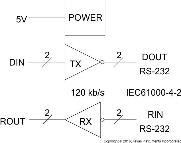
3 Description
The TRS202E consists of two line drivers, two line
receivers, and a dual charge-pump circuit. TRS202E has IEC61000-4-2 (Level 4) ESD
protection pin-to-pin (serial-port connection pins, including GND). The device meets
the requirements of TIA/EIA-232-F and provides the electrical interface between an
asynchronous communication controller and the serial-port connector. The charge pump
and four small external capacitors allow operation from a single 5V supply. The
device operates at data signaling rates up to 120kbit/s and a maximum of
30V/µs driver output slew rate.
| PART NUMBER | PACKAGE(1) | PACKAGE SIZE(2) |
|---|---|---|
| TRS202E | SOIC (D) (16) | 9.9mm × 6mm |
| SOIC (DW) (16) | 10.4mm × 10.3mm | |
| PDIP (N) (16) | 19.3mm × 9.4mm | |
| TSSOP (PW) (16) | 5mm x 6.4mm |
 Logic Diagram (Positive Logic)