SCDS248E October 2009 – September 2022 TS12A12511
PRODUCTION DATA
- 1 Features
- 2 Applications
- 3 Description
- 4 Revision History
- 5 Pin Configuration and Functions
- 6 Specifications
- 7 Parameter Measurement Information
- 8 Detailed Description
- 9 Application and Implementation
- 10Power Supply Recommendations
- 11Layout
- 12Device and Documentation Support
- 13Mechanical, Packaging, and Orderable Information
Package Options
Mechanical Data (Package|Pins)
Thermal pad, mechanical data (Package|Pins)
Orderable Information
3 Description
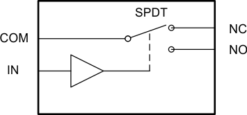
The TS12A12511 is a bidirectional, single-channel, single-pole double-throw (SPDT) analog switch that can pass signals with swings of 0 to 12 V or –6 V to 6 V. This switch conducts equally well in both directions when it is on. The device also offers a low ON-state resistance of 5 Ω (typical), which is matched to within 1 Ω between channels. The maximum current consumption is <1 μA and –3 dB bandwidth is >93 MHz. The TS12A12511 exhibits break-before-make switching action, preventing momentary shorting when switching channels. This device is available packaged in an 8-lead VSSOP, 8-lead SOT-23, and a 8-pin WSON.
| PART NUMBER | PACKAGE | BODY SIZE (NOM) |
|---|---|---|
| TS12A12511 | DCN (SOT-23, 8) | 2.90 mm × 1.63 mm |
| DGK (VSSOP, 8) | 3.00 mm × 3.00 mm | |
| DRJ (WSON, 8) | 4.00 mm × 4.00 mm |
 Simplified Schematic