SLOS489D December 2005 – May 2018 TS321
PRODUCTION DATA.
- 1 Features
- 2 Applications
- 3 Description
- 4 Revision History
- 5 Pin Configuration and Functions
- 6 Specifications
- 7 Detailed Description
- 8 Application and Implementation
- 9 Power Supply Recommendations
- 10Layout
- 11Device and Documentation Support
Package Options
Mechanical Data (Package|Pins)
Thermal pad, mechanical data (Package|Pins)
Orderable Information
7.3.5 Stability With High Capacitive Loads
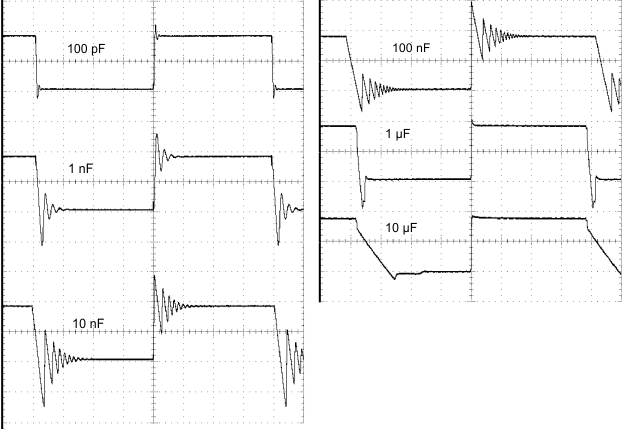
Operational amplifiers have reduced phase margin when there is a direct capacitance on the output. The stability is affected most when the amplifier is set to unity gain. Small signal response to a step input of 100 mV reveals the loop stability with a range of capacitors. See SLVA381 to correlate response waveform to phase margin. The responses at 1 nF or less indicate acceptable phase margin. The responses at 1 uF and above indicate good phase margin.
 Figure 7. Small-Signal Response