SCDS208B JUNE 2007 – October 2016 TS3A24157
PRODUCTION DATA.
- 1 Features
- 2 Applications
- 3 Description
- 4 Revision History
- 5 Pin Configuration and Functions
- 6 Specifications
- 7 Parameter Measurement Information
- 8 Detailed Description
- 9 Application and Implementation
- 10Power Supply Recommendations
- 11Layout
- 12Device and Documentation Support
- 13Mechanical, Packaging, and Orderable Information
Package Options
Refer to the PDF data sheet for device specific package drawings
Mechanical Data (Package|Pins)
- RSE|10
- DGS|10
Thermal pad, mechanical data (Package|Pins)
Orderable Information
1 Features
- Specified Break-Before-Make Switching
- Low ON-State Resistance (0.65-Ω Maximum)
- Low Charge Injection
- Excellent ON-State Resistance Matching
- Low Total Harmonic Distortion
- 1.65-V to 3.6-V Single-Supply Operation
- Bidirectional Signal Paths
- Latch-Up Performance Exceeds 100 mA Per JESD 78, Class II
- ESD Performance Tested Per JESD 22
- 2000-V Human-Body Model
(A114-B, Class II) - 1000-V Charged-Device Model (C101)
- 2000-V Human-Body Model
2 Applications
- Cell Phones
- PDAs
- Portable Instrumentation
- Audio and Video Signal Routing
- Low-Voltage Data Acquisition Systems
- Communication Circuits
- Modems
- Hard Drives
- Computer Peripherals
- Wireless Terminals and Peripherals
3 Description
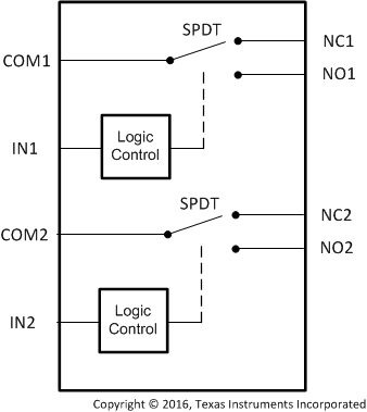
The TS3A24157 is a bidirectional, 2-channel, single-pole double-throw (SPDT) analog switch that is designed to operate from 1.65 V to 3.6 V. The device offers low ON-state resistance and excellent ON-state resistance matching with the break-before-make feature, to prevent signal distortion during the transfer of a signal from one channel to another. The device has excellent total harmonic distortion (THD) performance and consumes very-low power. These features make this device suitable for portable audio applications.
Device Information(1)
| PART NUMBER | PACKAGE | BODY SIZE (NOM) |
|---|---|---|
| TS3A24157 | UQFN (10) | 1.50 mm × 2.00 mm |
| VSSOP (10) | 3.00 mm × 3.00 mm |
- For all available packages, see the orderable addendum at the end of the data sheet.
Functional Block Diagram
