SCDS337F December   2012  – June 2019 TS3USB3000

PRODUCTION DATA.  

  1. Features
  2. Applications
  3. Description
    1.     Device Images
      1.      Functional Block Diagram
  4. Revision History
  5. Pin Configuration and Functions
    1.     Pin Functions
  6. Specifications
    1. 6.1 Absolute Maximum Ratings
    2. 6.2 ESD Ratings
    3. 6.3 Recommended Operating Conditions
    4. 6.4 Thermal Information
    5. 6.5 Electrical Characteristics
    6. 6.6 Dynamic Characteristics
    7. 6.7 Timing Requirements
    8. 6.8 Typical Characteristics
  7. Parameter Measurement Information
  8. Detailed Description
    1. 8.1 Overview
    2. 8.2 Functional Block Diagram
    3. 8.3 Feature Description
      1. 8.3.1 Low Power Mode
      2. 8.3.2 Overvoltage Protection When 9-V Short to D+/– Pin
      3. 8.3.3 Pin Leakage
    4. 8.4 Device Functional Modes
      1. 8.4.1 High Impedance Mode
  9. Application and Implementation
    1. 9.1 Application Information
    2. 9.2 Typical Application
      1. 9.2.1 Design Requirements
      2. 9.2.2 Detailed Design Procedure
      3. 9.2.3 Application Curves
  10. 10Power Supply Recommendations
  11. 11Layout
    1. 11.1 Layout Guidelines
    2. 11.2 Layout Example
  12. 12Device and Documentation Support
    1. 12.1 Documentation Support
      1. 12.1.1 Related Documentation
    2. 12.2 Receiving Notification of Documentation Updates
    3. 12.3 Community Resources
    4. 12.4 Trademarks
    5. 12.5 Electrostatic Discharge Caution
    6. 12.6 Glossary
  13. 13Mechanical, Packaging, and Orderable Information
    1. 13.1 Package Option Addendum
      1. 13.1.1 Packaging Information

Package Options

Mechanical Data (Package|Pins)
Thermal pad, mechanical data (Package|Pins)
Orderable Information

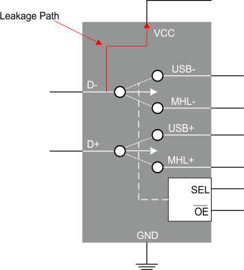
Pin Leakage

When the voltage on the D+/– pins rises above VCC +1 V a leakage path in the device starts conducting as shown in Figure 14. The amount of leakage depends on the VCC voltage and the pin voltage. This leakage is governed by Equation 1:

Equation 1. TS3USB3000 eq_1_SCDS337.gif
TS3USB3000 application_2.gifFigure 14. Potential Leakage Path D+/– to VCC