SCDS174D August 2004 – November 2015 TS5A3159
PRODUCTION DATA.
- 1 Features
- 2 Applications
- 3 Description
- 4 Revision History
- 5 Pin Configuration and Functions
-
6 Specifications
- 6.1 Absolute Maximum Ratings
- 6.2 ESD Ratings
- 6.3 Recommended Operating Conditions
- 6.4 Thermal Information
- 6.5 Electrical Characteristics for 5-V Supply
- 6.6 Electrical Characteristics for 3.3-V Supply
- 6.7 Electrical Characteristics for 2.5-V Supply
- 6.8 Electrical Characteristics for 1.8-V Supply
- 6.9 Switching Characteristics for 5-V Supply
- 6.10 Switching Characteristics for 3.3-V Supply
- 6.11 Switching Characteristics for 2.5-V Supply
- 6.12 Switching Characteristics for 1.8-V Supply
- 6.13 Typical Characteristics
- 7 Parameter Measurement Information
- 8 Detailed Description
- 9 Application and Implementation
- 10Power Supply Recommendations
- 11Layout
- 12Device and Documentation Support
- 13Mechanical, Packaging, and Orderable Information
Package Options
Mechanical Data (Package|Pins)
Thermal pad, mechanical data (Package|Pins)
Orderable Information
8 Detailed Description
8.1 Overview
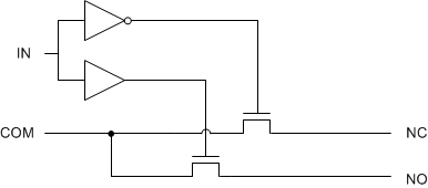
The TS5A3159 is a single-pole-double-throw (SPDT) solid-state analog switch. The TS5A3159, like all analog switches, is bidirectional. When powered on, each COM pin is connected to the NC pin. For this device, NC stands for normally closed and NO stands for normally open. If IN is low, COM is connected to NC. If IN is high, COM is connected to NO.
The TS5A3159 is a break-before-make switch. This means that during switching, a connection is broken before a new connection is established. The NC and NO pins are never connected to each other.
8.2 Functional Block Diagram

8.3 Feature Description
The low ON-state resistance, ON-state resistance matching, and charge injection in the TS5A3159 make this switch an excellent choice for analog signals that require minimal distortion. In addition, the low THD allows audio signals to be preserved more clearly as they pass through the device.
The 1.65-V to 5.5-V operation allows compatibility with more logic levels, and the bidirectional I/Os can pass analog signals from 0 V to V+ with low distortion.
8.4 Device Functional Modes
Table 1. Function Table
| IN | NC TO COM, COM TO NC |
NO TO COM, COM TO NO |
|---|---|---|
| L | ON | OFF |
| H | OFF | ON |