SCDS241B May 2008 – December 2016 TS5A9411
PRODUCTION DATA.
- 1 Features
- 2 Applications
- 3 Description
- 4 Revision History
- 5 Pin Configuration and Functions
- 6 Specifications
- 7 Parameter Measurement Information
- 8 Detailed Description
- 9 Application and Implementation
- 10Power Supply Recommendations
- 11Layout
- 12Device and Documentation Support
- 13Mechanical, Packaging, and Orderable Information
Package Options
Mechanical Data (Package|Pins)
- DCK|6
Thermal pad, mechanical data (Package|Pins)
Orderable Information
7 Parameter Measurement Information
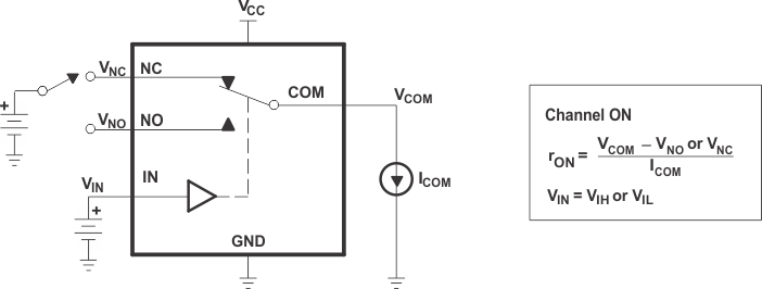 Figure 5. ON-State Resistance
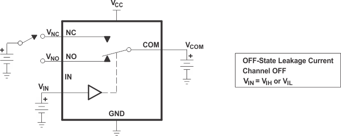
INC(OFF), INC(PWROFF), INO(OFF), INO(PWROFF), ICOM(OFF), ICOM(PWROFF)
Figure 6. OFF-State Leakage Current
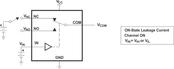
ICOM(ON), INC(ON), INO(ON)
Figure 7. ON-State Leakage Current
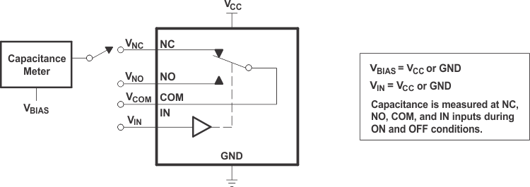
CI, CCOM(ON), CNC(OFF), CNO(OFF), CNC(ON), CNO(ON)
Figure 8. Capacitance
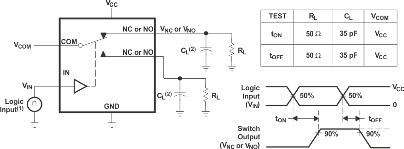
1. All input pulses are supplied by generators having the following characteristics:
- PRR ≤ 10 MHz
- ZO = 50 Ω
- tr < 5 ns
- tf < 5 ns
2. CL includes probe and jig capacitance.
Figure 9. Turnon and Turnoff Time

1. All input pulses are supplied by generators having the following characteristics:
- PRR ≤ 10 MHz
- ZO = 50 Ω
- tr < 5 ns
- tf < 5 ns
2. CL includes probe and jig capacitance.
Figure 10. Break-Before-Make Time
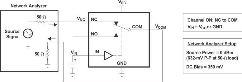 Figure 11. Bandwidth
 Figure 12. OFF Isolation
 Figure 13. Crosstalk

1. All input pulses are supplied by generators having the following characteristics:
- PRR ≤ 10 MHz
- ZO = 50 Ω
- tr < 5 ns
- tf < 5 ns
2. CL includes probe and jig capacitance.
Figure 14. Charge Injection
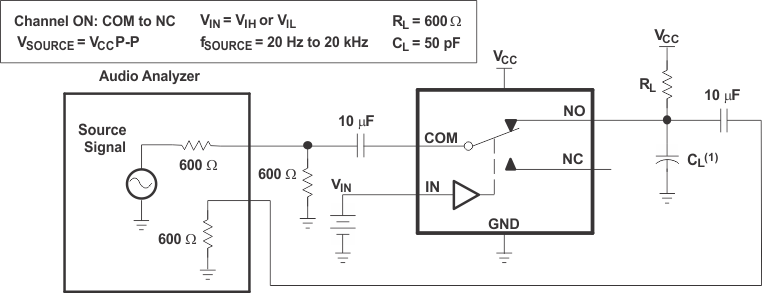
1. CL includes probe and jig capacitance.
Figure 15. Total Harmonic Distortion