SBAS545A September 2011 – December 2016 TSC2007-Q1
PRODUCTION DATA.
- 1 Features
- 2 Applications
- 3 Description
- 4 Revision History
- 5 Pin Configuration and Functions
-
6 Specifications
- 6.1 Absolute Maximum Ratings
- 6.2 ESD Ratings
- 6.3 Recommended Operating Conditions
- 6.4 Thermal Information
- 6.5 Electrical Characteristics
- 6.6 Timing Requirements: Standard Mode (SCL = 100 kHz)
- 6.7 Timing Requirements: Fast Mode (SCL = 400 kHz)
- 6.8 Timing Requirements: High-Speed Mode (SCL = 1.7 MHz)
- 6.9 Timing Requirements: High-Speed Mode (SCL = 3.4 MHz)
- 6.10 Typical Characteristics
- 7 Detailed Description
- 8 Application and Implementation
- 9 Power Supply Recommendations
- 10Layout
- 11Device and Documentation Support
- 12Mechanical, Packaging, and Orderable Information
Package Options
Mechanical Data (Package|Pins)
- PW|16
Thermal pad, mechanical data (Package|Pins)
Orderable Information
8 Application and Implementation
NOTE
Information in the following applications sections is not part of the TI component specification, and TI does not warrant its accuracy or completeness. TI’s customers are responsible for determining suitability of components for their purposes. Customers should validate and test their design implementation to confirm system functionality.
8.1 Application Information
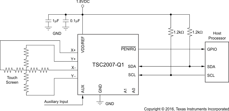
The TSC2007-Q1 is designed for use in automotive touch-screen displays. It supports resistive 4-wire touch screens that can be used in the head unit for infotainment and navigation displays. The auxiliary input can be used for external temperature sensing, ambient light monitoring for back-lighting control, or for current monitoring.
8.2 Typical Application
A typical application of the TSC2007-Q1 is shown in Figure 34.
 Figure 34. Typical Circuit Configuration
8.2.1 Design Requirements
The system-level requirements for this design include:
- Normal 4-wire resistive touch screen
- To achieve the best SNR, select the highest operating voltage of the TSC2007-Q1 device that is compatible with the system.
8.2.2 Detailed Design Procedure
8.2.2.1 4-Wire Touch Screen Coordinate Pair Measurement
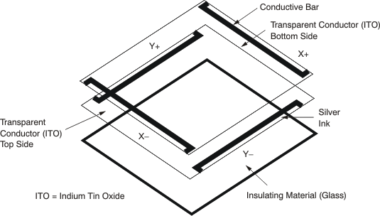
A 4-wire touch screen is typically constructed as shown in Figure 35. It consists of two transparent resistive layers separated by insulating spacers.
 Figure 35. 4-Wire Touch Screen Construction
The 4-wire touch screen panel works by applying a voltage across the vertical or horizontal resistive network. The A-D converter converts the voltage measured at the point where the panel is touched. A measurement of the Y position of the pointing device is made by connecting the X+ input to a data converter chip, turning on the Y+ and Y– drivers, and digitizing the voltage seen at the X+ input. The voltage measured is determined by the voltage divider developed at the point of touch. For this measurement, the horizontal panel resistance in the X+ lead does not affect the conversion because of the high input impedance of the A-D converter.
Voltage is then applied to the other axis, and the A-D converter converts the voltage representing the X position on the screen. This process provides the X and Y coordinates to the associated processor.
Measuring touch pressure (Z) can also be done with the TSC2007-Q1. To determine pen or finger touch, the pressure of the touch must be determined. Generally, it is not necessary to have very high performance for this test; therefore, 8-bit resolution mode may be sufficient (however, data sheet calculations are shown using the
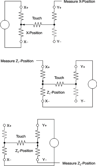
12-bit resolution mode). There are several different ways of performing this measurement. The TSC2007-Q1 supports two methods. The first method requires knowing the X-plate resistance, the measurement of the X position, and two additional cross panel measurements (Z2 and Z1) of the touch screen (see Figure 36). Equation 3 calculates the touch resistance:

The second method requires knowing both the X-plate and Y-plate resistance, measurement of X position and Y position, and Z1. Equation 4 also calculates the touch resistance:

 Figure 36. Pressure Measurement
When the touch panel is pressed or touched and the drivers to the panel are turned on, the voltage across the touch panel often overshoots and then slowly settles down (decays) to a stable DC value. This effect is a result of mechanical bouncing caused by vibration of the top layer sheet of the touch panel when the panel is pressed. This settling time must be accounted for, or else the converted value is incorrect. Therefore, a delay must be introduced between the time the driver for a particular measurement is turned on, and the time a measurement is made.
In some applications, external capacitors may be required across the touch screen for filtering noise picked up by the touch screen (noise generated by the LCD panel or back-light circuitry). The value of these capacitors provides a low-pass filter to reduce the noise, but creates an additional settling time requirement when the panel is touched. The settling time typically shows up as gain error.
To solve this problem, the TSC2007-Q1 can be commanded to turn on the drivers only, without performing a conversion. Time can then be allowed to perform a conversion before the command is issued.
The TSC2007-Q1 touch screen interface can measure position (X, Y) and pressure (Z).
8.2.2.2 Touch-Panel Driving Power
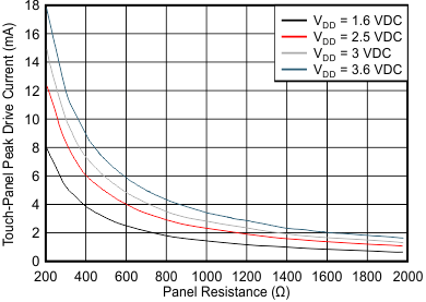
On a resistive touch-screen system, the driving current of the touch panel, provided by the TSC device through the analog interface, has the highest impact on the power consumption in the touch screen system. This touch-panel power consumption is decided by the resistance of the touch panel and the TSC power-supply (VDD) voltage. Figure 37 shows this relationship. The touch screen is driven by the TSC from the VDD supply and the resistance of the panel determines the peak drive current.
Figure 37 only shows the ideal TSC driving condition where the internal resistance of the TSC is ignored because the resistance is small (5 to 6 Ω) compared to the resistance of the touch panel (hundreds to thousands of Ω). Therefore the actual power consumption may be less than that shown in Figure 37.
A user can reduce power consumption in three ways:
- Using touch screens with higher resistance
- Using a low-power supply (VDD) to the TSC
- Reducing the driver on-time or the on-off ratio of the driver
Touch panels with higher resistance are likely to cause more noise and longer settling time which limits the options for users.
The TSC2007-Q1 device is designed with a power supply (VDD) range from 1.2 V to 3.6 V.
8.2.3 Application Curve
 Figure 37. Touch-Panel Power Consumption