SCDS335A September 2012 – August 2014 TSU8111
PRODUCTION DATA.
- 1 Features
- 2 Applications
- 3 Description
- 4 Revision History
- 5 Pin Configuration and Functions
- 6 Specifications
-
7 Detailed Description
- 7.1 Overview
- 7.2 Functional Block Diagram
- 7.3 Feature Description
- 7.4 Device Functional Modes
- 7.5 Programming
- 7.6
Register Map
- 7.6.1 Device ID (01h) Register Field Descriptions
- 7.6.2 Control (02h) Register Field Descriptions
- 7.6.3 Interrupt 1 (03h) Register Field Descriptions
- 7.6.4 Interrupt 2 (04h) Register Field Descriptions
- 7.6.5 Interrupt Mask 1 (05h) Register Field Descriptions
- 7.6.6 Interrupt Mask 2 (06h) Register Field Descriptions
- 7.6.7 ADC (07h) Register Field Descriptions
- 7.6.8 Timing Set 1 (08h) Register Field Descriptions
- 7.6.9 Timing Set 2 (09h) Register Field Descriptions
- 7.6.10 Device Type 1 (0Ah) Register Field Descriptions
- 7.6.11 Device Type 2 (0Bh) Register Field Descriptions
- 7.6.12 Button 1 (0Ch) Register Field Descriptions
- 7.6.13 Button 2 (0Dh) Register Field Descriptions
- 7.6.14 Manual SW 1 (13h) Register Field Descriptions
- 7.6.15 Manual SW 2 (14h) Register Field Descriptions
- 7.6.16 Reset (1Bh) Register Field Descriptions
- 7.6.17 Charger control 1 (20h) Register Field Descriptions
- 7.6.18 Charger control 2 (21h) Register Field Descriptions
- 7.6.19 Battery Charger Control 3 (22h) Register Field Descriptions
- 7.6.20 Charger Interrupt (24h) Register Field Descriptions
- 7.6.21 Charger Interrupt Mask (25h) Register Field Descriptions
- 7.6.22 Charger Status (26h) Register Field Descriptions
- 8 Application and Implementation
- 9 Power Supply Recommendations
- 10Layout
- 11Device and Documentation Support
- 12Mechanical, Packaging, and Orderable Information
Package Options
Mechanical Data (Package|Pins)
- YFP|20
Thermal pad, mechanical data (Package|Pins)
Orderable Information
6 Specifications
6.1 Absolute Maximum Ratings
over operating free-air temperature range (unless otherwise noted) (1)| MIN | MAX | UNIT | |||
|---|---|---|---|---|---|
| Supply voltage | VBAT | –0.5 | 6 | V | |
| VBUS | –0.5 | 28 | |||
| VDDIO | –0.5 | 4.6 | |||
| Input-output terminal voltage, VIO | VDM_CON, VDP_CON, VID_CON, VDP_HT, VDM_HT | –0.5 | VBAT + 0.5(2) | V | |
| VRxD, VTxD | –0.5 | VBAT + 0.5(2) | |||
| VSDA | –0.5 | 4.6 | |||
| Output voltage | VLDO | –0.5 | 6 | V | |
| VJIG | –0.5 | VBAT + 0.5(2) | |||
| VINTB, VBOOT | –0.5 | 4.6 | |||
| Input current | IBAT | 1 | A | ||
| IBUS | 1 | ||||
| IK | Analog port diode current | –50 | 50 | mA | |
| IIK | Digital logic input clamp current | –50 | |||
| ISCL | –50 | 50 | |||
| Input-output terminal current, IIO | ISDA | –50 | 50 | mA | |
| IIO(on) | On-state continuous switch current | –60 | 60 | ||
| IIO(peak) | On-state peak switch current | –150 | 150 | ||
| Output current | ILDO | 100 | mA | ||
| IGND | |||||
| IINTB, IBOOT | –50 | 50 | |||
(1) Stresses beyond those listed under Absolute Maximum Ratings may cause permanent damage to the device. These are stress ratings only, which do not imply functional operation of the device at these or any other conditions beyond those indicated under Recommended Operating Conditions. Exposure to absolute-maximum-rated conditions for extended periods may affect device reliability.
(2) If VBUS is present without VBAT, then the absolute maximum voltage is VBUS + 0.5 V, and shall not exceed 6 V in total.
6.2 Handling Ratings
| MIN | MAX | UNIT | ||||
|---|---|---|---|---|---|---|
| Tstg | Storage temperature range | –65 | 150 | °C | ||
| V(ESD) | Electrostatic discharge | Human body model (HBM), stress voltage(1) | VBUS, DP_CON, DM_CON, ID_CON | –12 | 12 | kV |
| Charged device model (CDM), stress voltage(2) | All other pins | –2 | 2 | |||
| IEC-61000-4-2 contact discharge | –4 | 4 | kV | |||
(1) JEDEC document JEP155 states that 500-V HBM allows safe manufacturing with a standard ESD control process.
(2) JEDEC document JEP157 states that 250-V CDM allows safe manufacturing with a standard ESD control process.
6.3 Recommended Operating Conditions
over operating free-air temperature range (unless otherwise noted)| MIN | MAX | UNIT | ||
|---|---|---|---|---|
| Supply voltage | VBAT | 3 | 4.4 | V |
| VBUS | 4 | 6.5 | ||
| VDDIO | 1.65 | 3.6 | ||
| Input-output terminal voltage, VIO | VDM_CON, VDP_CON, VID_CON, VDP_HT, VDM_HT, VRxD, VTxD | 0 | 3.6 | V |
| ID pin capacitance | CID | 1 | nF | |
| LDO output capacitance | CLDO | 1 | ||
| Operating free-air temperature | TA | –40 | 85 | °C |
6.4 Thermal Information
| THERMAL METRIC(1) | TSU8111 | UNIT | |
|---|---|---|---|
| YFP | |||
| 20 PINS | |||
| RθJA | Junction-to-ambient thermal resistance | 70.3 | °C/W |
| RθJC(top) | Junction-to-case (top) thermal resistance | 0.4 | |
| RθJB | Junction-to-board thermal resistance | 10.4 | |
| ψJT | Junction-to-top characterization parameter | 1.8 | |
| ψJB | Junction-to-board characterization parameter | 10.4 | |
(1) For more information about traditional and new thermal metrics, see the IC Package Thermal Metrics application report, SPRA953.
6.5 Electrical Characteristics
VBAT = 3 V to 4.4 V, VDDIO = 2.8 V, TA = –40°C to 85°C (unless otherwise noted)| PARAMETER | TEST CONDITIONS | MIN | TYP | MAX | UNIT | ||
|---|---|---|---|---|---|---|---|
| USB and UART PATHS(1) | |||||||
| RON | On-state resistance | VI = 0 V to 3.6 V, IO = –2 mA, VBAT = 3.6 V | 8 | Ω | |||
| ΔRON | On-state resistance match between channels | VI = 0.4 V, IO = –2 mA, VBAT = 3.6 V | 0.5 | Ω | |||
| RON(flat) | On-state resistance flatness | VI = 0 V to 3.6 V, IO = –2 mA, VBAT = 3.6 V | 0.7 | Ω | |||
| IIO(OFF) | Off-state leakage current | VI = 0.3 V, VO = 2.7 V or VI = 2.7 V, VO = 0.3 V, VBAT = 4.4 V, Switch off | 45 | nA | |||
| IIO(ON) | On-state leakage current | VI = OPEN, VO = 0.3 V or 2.7 V, VBAT = 4.4 V, Switch on | 50 | nA | |||
| CI(OFF) | Off-state capacitance at input | DC bias = 0 V or 3.6 V, f = 10 MHz, Switch off | 4 | pF | |||
| CO(OFF) | Off-state capacitance at output | DC bias = 0 V or 3.6 V, f = 10 MHz, Switch off | 7.5 | pF | |||
| CI(ON) | On-state capacitance at input | DC bias = 0 V or 3.6 V, f = 10 MHz, Switch off | 8.6 | pF | |||
| CO(ON) | On-state capacitance at output | DC bias = 0 V or 3.6 V, f = 10 MHz, Switch off | 8.6 | pF | |||
| BW | Bandwidth | RL = 50 Ω, Switch on | 820 | MHz | |||
| OISO | Off isolation | f = 240 MHz, RL = 50 Ω, Switch off | -36 | dB | |||
| XTALK | Crosstalk | f = 240 MHZ, RL = 50 Ω | -35 | dB | |||
| LINEAR CHARGER(2) | |||||||
| VCHG(OK) | Charger input voltage OK threshold | VBUS – VBAT | Rising | 250 | mV | ||
| Falling | 45 | ||||||
| VBUS(OVP) | VBUS over-voltage protection (default 7.5 V) | I2C register 22h [7:6] = 00 | 6 | V | |||
| I2C register 22h [7:6] = 01 | 6.5 | ||||||
| I2C register 22h [7:6] = 10 | 7 | ||||||
| I2C register 22h [7:6] = 11 | 7.5 | ||||||
| VBUS(OVP,fail) | VBUS over-voltage falling threshold for restart charging | 320 | mV | ||||
| VPRECHG | Pre-charge threshold voltage | 2.5 | V | ||||
| VCHG(RST) | Charge restart threshold (default 100 mV) | I2C register 20h [6:5] = 00 | 130 | mV | |||
| I2C register 20h [6:5] = 01 | 130 | ||||||
| I2C register 20h [6:5] = 10 | 190 | ||||||
| I2C register 20h [6:5] = 11 | 240 | ||||||
| VDO(LDO) | LDO dropout voltage | VBUS = 4.5 V, ILDO = 50 mA | 150 | mV | |||
| VLDO | LDO output voltage | VLDO + VDO(LDO) ≤ VBUS ≤ VBUS(OVP) | 4.9 | V | |||
| ILDO | LDO output current | VLDO = 0 V | 50 | mA | |||
| IPRECHG | Default pre-charge current | VBAT = 2 V | 90 | mA | |||
| CLDO | LDO output capacitance | 1 | μF | ||||
| TPRECHG | Pre-charge timeout | 30 | min | ||||
| VSET | Charging voltage | I2C register 21h [3:0] = 0000 | 4 | V | |||
| I2C register 21h [3:0] = 0001 | 4.02 | ||||||
| I2C register 21h [3:0] = 0010 | 4.04 | ||||||
| I2C register 21h [3:0] = 0011 | 4.06 | ||||||
| I2C register 21h [3:0] = 0100 | 4.08 | ||||||
| I2C register 21h [3:0] = 0101 | 4.1 | ||||||
| I2C register 21h [3:0] = 0110 | 4.12 | ||||||
| I2C register 21h [3:0] = 0111 | 4.14 | ||||||
| I2C register 21h [3:0] = 1000 | 4.16 | ||||||
| I2C register 21h [3:0] = 1001 | 4.18 | ||||||
| I2C register 21h [3:0] = 1010 (default) | 4.2 | ||||||
| I2C register 21h [3:0] = 1011 | 4.22 | ||||||
| I2C register 21h [3:0] = 1100 | 4.24 | ||||||
| I2C register 21h [3:0] = 1101 | 4.26 | ||||||
| I2C register 21h [3:0] = 1110 | 4.28 | ||||||
| I2C register 21h [3:0] = 1111 | 4.35 | ||||||
| ISET | Fast charging current | I2C register 22h [3:0] = 0000 | 200 | mA | |||
| I2C register 22h [3:0] = 0001 | 250 | ||||||
| I2C register 22h [3:0] = 0010 | 300 | ||||||
| I2C register 22h [3:0] = 0011 | 350 | ||||||
| I2C register 22h [3:0] = 0100 | 400 | ||||||
| I2C register 22h [3:0] = 0101 (default) | 450 | ||||||
| I2C register 22h [3:0] = 0110 | 500 | ||||||
| I2C register 22h [3:0] = 0111 | 550 | ||||||
| I2C register 22h [3:0] = 1000 | 600 | ||||||
| I2C register 22h [3:0] = 1001 | 650 | ||||||
| I2C register 22h [3:0] = 1010 | 700 | ||||||
| I2C register 22h [3:0] = 1011 | 750 | ||||||
| I2C register 22h [3:0] = 1100 | 800 | ||||||
| I2C register 22h [3:0] = 1101 | 850 | ||||||
| I2C register 22h [3:0] = 1110 | 900 | ||||||
| I2C register 22h [3:0] = 1111 | 950 | ||||||
| Charging current accuracy | -8% | 8% | |||||
| IFULL | Full charge current | I2C register 22h [7:4] = 0000 | 50 | mA | |||
| I2C register 22h [7:4] = 0001 | 60 | ||||||
| I2C register 22h [7:4] = 0010 | 70 | ||||||
| I2C register 22h [7:4] = 0011 | 80 | ||||||
| I2C register 22h [7:4] = 0100 | 90 | ||||||
| I2C register 22h [7:4] = 0101 (default) | 100 | ||||||
| I2C register 22h [7:4] = 0110 | 110 | ||||||
| I2C register 22h [7:4] = 0111 | 120 | ||||||
| I2C register 22h [7:4] = 1000 | 130 | ||||||
| I2C register 22h [7:4] = 1001 | 140 | ||||||
| I2C register 22h [7:4] = 1010 | 150 | ||||||
| I2C register 22h [7:4] = 1011 | 160 | ||||||
| I2C register 22h [7:4] = 1100 | 170 | ||||||
| I2C register 22h [7:4] = 1101 | 180 | ||||||
| I2C register 22h [7:4] = 1110 | 190 | ||||||
| I2C register 22h [7:4] = 1111 | 200 | ||||||
| I2C INTERFACE (SCL and SDA) | |||||||
| VIH | High-level input voltage | VDDIO × 0.7 | VDDIO | V | |||
| VIL | Low-level input voltage | 0 | VDDIO × 0.3 | V | |||
| VOH | High-level output voltage | IOH = –3 mA | VDDIO × 0.7 | VDDIO | V | ||
| VOL | Low-level output voltage | IOL = 3 mA | 0 | 0.4 | V | ||
| DIGITAL SIGNAL OUTPUTS – JIG, INTB, and BOOT | |||||||
| VOL(JIG) | Low-level output voltage | IOL = 10 mA, VBAT = 3.0 V | 0.5 | V | |||
| VOH(INTB,BOOT) | High-level output voltage | IOH = -4 mA, VDDIO = 1.65 V | 1.16 | VDDIO | V | ||
| VOL(INTB,BOOT) | Low-level output voltage | IOL = 4 mA, VDDIO = 1.65 V | 0 | 0.33 | V | ||
| CURRENT CONSUMPTION | |||||||
| IBAT(standby) | VBAT standby current consumption | VBUS = 0 V, idle state | 27 | 36 | μA | ||
| IBAT(operating) | VBAT operating current consumption | VBUS = 0 V, USB switch closed | 100 | 150 | μA | ||
| IBUS | VBUS operating current consumption | VBUS = 5 V, VBAT floating | 0.6 | 0.75 | mA | ||
| VOLTAGE PROTECTION | |||||||
| VBUS(UVLO) | VBUS under voltage – upper threshold | VBUS rising | 2.85 | V | |||
| VBUS under voltage – lower threshold | VBUS falling | 2.55 | |||||
| VBUS(valid) | VBUS interrupt threshold | VBUS rising | 3.6 | V | |||
| VBAT(UVLO) | VBAT under voltage – upper threshold | VBAT rising | 2.65 | V | |||
| VBAT under voltage – lower threshold | VBAT falling | 2.45 | |||||
(1) VO is equal to the asserted voltage on DP_CON and DM_CON. VI is equal to the asserted voltage on DP_HT and DM_HT pins. IO is equal to the current out of the DP_CON and DM_CON pins. II is equal to the current into the DP_HT and DM_HT pins.
(2) Fast charging current will fall below listed values when junction temperature rises above 85°C due to thermal regulation circuitry.
6.6 Timing Requirements
| MIN | TYP | MAX | UNIT | ||
|---|---|---|---|---|---|
| fSCL | I2C clock frequency | 64 | 400 | kHz | |
6.7 Switching Characteristics
| PARAMETER | TEST CONDITIONS | MIN | TYP | MAX | UNIT | |
|---|---|---|---|---|---|---|
| ton | Switch turn-on time | From receipt of I2C ACK bit | 57 | µs | ||
| toff | Switch turn-off time | From receipt of I2C ACK bit | 5.2 | µs | ||
6.8 Typical Characteristics
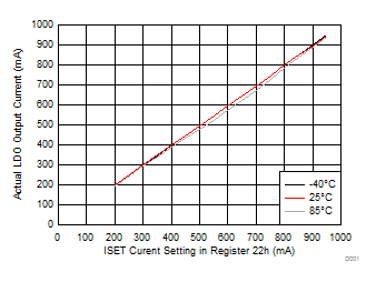
| VBAT = 4 V | VBUS = 5 V |
Register Setting Across Device Temperature Range