SLLSF15D August   2017  – May 2019 TUSB1042I

PRODUCTION DATA.  

  1. Features
  2. Applications
  3. Description
    1.     Device Images
      1.      Simplified Schematics
      2.      TUSB1042I Eye Diagram
  4. Revision History
  5. Pin Configuration and Functions
    1.     Pin Functions
  6. Specifications
    1. 6.1  Absolute Maximum Ratings
    2. 6.2  ESD Ratings
    3. 6.3  Recommended Operating Conditions
    4. 6.4  Thermal Information
    5. 6.5  Power Supply Characteristics
    6. 6.6  DC Electrical Characteristics
    7. 6.7  AC Electrical Characteristics
    8. 6.8  DCI Specific Electrical Characteristics
    9. 6.9  Timing Requirements
    10. 6.10 Switching Characteristics
    11. 6.11 Typical Characteristics
  7. Parameter Measurement Information
  8. Detailed Description
    1. 8.1 Overview
    2. 8.2 Functional Block Diagram
    3. 8.3 Feature Description
      1. 8.3.1 USB 3.1
      2. 8.3.2 4-level Inputs
      3. 8.3.3 Receiver Linear Equalization
    4. 8.4 Device Functional Modes
      1. 8.4.1 Device Configuration in GPIO Mode
      2. 8.4.2 Device Configuration In I2C Mode
      3. 8.4.3 Linear EQ Configuration
      4. 8.4.4 USB3.1 Modes
      5. 8.4.5 Operation Timing – Power Up
    5. 8.5 Programming
    6. 8.6 Register Maps
      1. 8.6.1 General Register (address = 0x0A) [reset = 00000001]
        1. Table 9. General Registers
      2. 8.6.2 USB3.1 Control/Status Registers (address = 0x20) [reset = 00000000]
        1. Table 10. USB3.1 Control/Status Registers (0x20)
      3. 8.6.3 USB3.1 Control/Status Registers (address = 0x21) [reset = 00000000]
        1. Table 11. USB3.1 Control/Status Registers (0x21)
      4. 8.6.4 USB3.1 Control/Status Registers (address = 0x22) [reset = 00000100]
        1. Table 12. USB3.1 Control/Status Registers (0x22)
  9. Application and Implementation
    1. 9.1 Application Information
    2. 9.2 Typical Application
      1. 9.2.1 Design Requirements
      2. 9.2.2 Detailed Design Procedure
      3. 9.2.3 Application Curve
    3. 9.3 System Examples
      1. 9.3.1 USB 3.1
  10. 10Power Supply Recommendations
  11. 11Layout
    1. 11.1 Layout Guidelines
    2. 11.2 Layout Example
  12. 12Device and Documentation Support
    1. 12.1 Related Links
    2. 12.2 Receiving Notification of Documentation Updates
    3. 12.3 Community Resources
    4. 12.4 Trademarks
    5. 12.5 Electrostatic Discharge Caution
    6. 12.6 Glossary
  13. 13Mechanical, Packaging, and Orderable Information

Package Options

Mechanical Data (Package|Pins)
Thermal pad, mechanical data (Package|Pins)
Orderable Information

Typical Characteristics

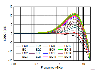
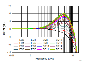
TUSB1042I D002_SLLSEV7.gif
Figure 1. USB RX EQ Settings Curves
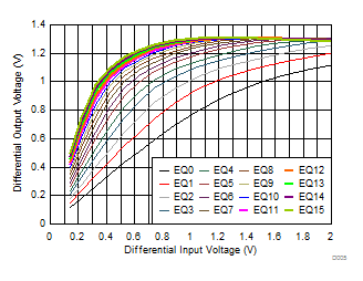
TUSB1042I D005_SLLSEW2.gif
Figure 3. USB TX Linearity Curves at 5 GHz
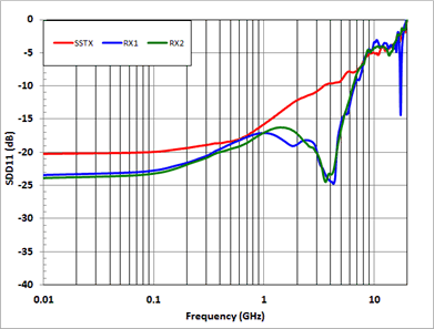
TUSB1042I Input_Return_Loss_SLLSF15.gif
Figure 5. Input Return Loss Performance
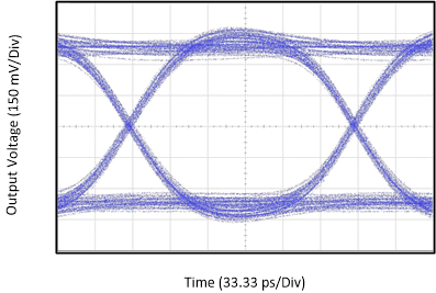
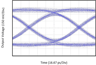
TUSB1042I TUSB1042_5G_Eye_SLLSF15.gif
Figure 7. USB 3.1 Gen1 Eye-Pattern Performance with 12-inch Input PCB Trace at 5 Gbps
TUSB1042I D003_SLLSEV7.gif
Figure 2. USB TX EQ Settings Curves
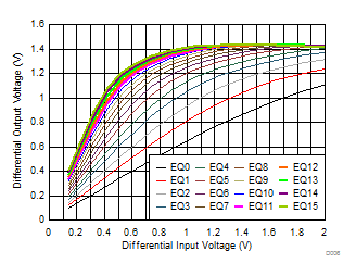
TUSB1042I D006_SLLSEW2.gif
Figure 4. USB RX Linearity Curves at 5 GHz
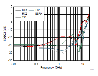
TUSB1042I D008_SLLSEV7.gif
Figure 6. Output Return Loss Performance
TUSB1042I TUSB1046A_DCI_10G_USB_Eye.gif
Figure 8. USB 3.1 Gen2 Eye-Pattern Performance with
12-inch Input PCB Trace at 10 Gbps