SLLS372I March 2000 – March 2017 TUSB2036
PRODUCTION DATA.
- 1 Features
- 2 Applications
- 3 Description
- 4 Revision History
- 5 Description (Continued)
- 6 Pin Configuration and Functions
- 7 Specifications
- 8 Detailed Description
- 9 Application and Implementation
- 10Power Supply Recommendations
- 11Layout
- 12Device and Documentation Support
- 13Mechanical, Packaging, and Orderable Information
Package Options
Mechanical Data (Package|Pins)
- VF|32
Thermal pad, mechanical data (Package|Pins)
Orderable Information
7 Specifications
7.1 Absolute Maximum Ratings
over operating free-air temperature range (unless otherwise noted)(1)| MIN | MAX | UNIT | |||
|---|---|---|---|---|---|
| VCC | Supply voltage(2) | –0.5 | 3.6 | V | |
| VI | Input voltage | –0.5 | VCC + 0.5 | V | |
| VO | Output voltage | –0.5 | VCC + 0.5 | V | |
| IIK | Input clamp current | VI < 0 V or VI < VCC | ±20 | mA | |
| IOK | Output clamp current | VO < 0 V or VO < VCC | ±20 | mA | |
| TA | Operating free-air temperature | 0 | 70 | °C | |
| Tstg | Storage temperature | –65 | 150 | °C | |
(1) Stresses beyond those listed under Absolute Maximum Ratings may cause permanent damage to the device. These are stress ratings only, and functional operation of the device at these or any other conditions beyond those indicated under Recommended Operating Conditions is not implied. Exposure to absolute-maximum-rated conditions for extended periods may affect device reliability.
(2) All voltage levels are with respect to GND.
7.2 ESD Ratings
| VALUE | UNIT | |||
|---|---|---|---|---|
| V(ESD) | Electrostatic discharge | Human body model (HBM), per ANSI/ESDA/JEDEC JS-001(1) | ±4000 | V |
| Charged-device model (CDM), per JEDEC specification JESD22-C101(2) | ±1500 | |||
(1) JEDEC document JEP155 states that 500-V HBM allows safe manufacturing with a standard ESD control process.
(2) JEDEC document JEP157 states that 250-V CDM allows safe manufacturing with a standard ESD control process.
7.3 Recommended Operating Conditions
| PARAMETER | MIN | NOM | MAX | UNIT | ||
|---|---|---|---|---|---|---|
| VCC | Supply voltage | 3 | 3.3 | 3.6 | V | |
| VI | Input voltage, TTL/LVCMOS(1) | 0 | VCC | V | ||
| VO | Output voltage, TTL/LVCMOS(2) | 0 | VCC | V | ||
| VIH(REC) | High-level input voltage, signal-ended receiver | 2 | VCC | V | ||
| VIL(REC) | Low-level input voltage, signal-ended receiver | 0.8 | V | |||
| VIH(TTL) | High-level input voltage, TTL/LVCMOS(1) | 2 | VCC | V | ||
| VIL(TTL) | Low-level input voltage, TTL/LVCMOS(1) | 0 | 0.8 | V | ||
| TA | Operating free-air temperature | 0 | 70 | °C | ||
| R(DRV) | External series, differential driver resistor | 22 (–5%) | 22 (+5%) | Ω | ||
| f(OPRH) | Operating (dc differential driver) full speed mode | 12 | Mb/s | |||
| f(OPRL) | Operating (dc differential driver) low speed mode | 1.5 | Mb/s | |||
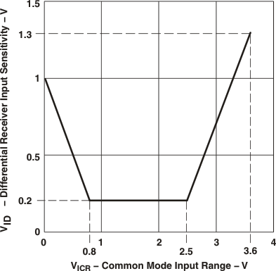
| VICR | Common mode, input range, differential receiver | 0.8 | 2.5 | V | ||
| tt | Input transition times, TTL/LVCMOS(1) | 0 | 25 | ns | ||
| TJ | Junction temperature range(3) | 0 | 115 | °C | ||
(1) Applies for input and bidirectional buffers.
(2) Applies for output and bidirectional buffers.
(3) These junction temperatures reflect simulated conditions. Absolute maximum junction temperature is 150°C. The customer is responsible for verifying junction temperature.
7.4 Thermal Information
| THERMAL METRIC(1) | TUSB2036 | UNIT | |
|---|---|---|---|
| VF (HLQFP) | |||
| 32 PINS | |||
| RθJA | Junction-to-ambient thermal resistance | 71.6 | °C/W |
| RθJC(top) | Junction-to-case (top) thermal resistance | 32.4 | °C/W |
| RθJB | Junction-to-board thermal resistance | 29.4 | °C/W |
| ψJT | Junction-to-top characterization parameter | 2.4 | °C/W |
| ψJB | Junction-to-board characterization parameter | 29.2 | °C/W |
(1) For more information about traditional and new thermal metrics, see the Semiconductor and IC Package Thermal Metrics application report, SPRA953.
7.5 Electrical Characteristics
over recommended ranges of operating free-air temperature and supply voltage (unless otherwise noted)| PARAMETER | TEST CONDITIONS | MIN | MAX | UNIT | ||
|---|---|---|---|---|---|---|
| VOH | High-level output voltage | TTL/LVCMOS | IOH = –4 mA | VCC – 0.5 | V | |
| USB data lines | R(DRV) = 15 kΩ to GND | 2.8 | ||||
| IOH = –12 mA (without R(DRV)) | VCC – 0.5 | |||||
| VOL | Low-level output voltage | TTL/LVCMOS | IOL = 4 mA | 0.5 | V | |
| USB data lines | R(DRV) = 1.5 kΩ to 3.6 V | 0.3 | ||||
| IOL = 12 mA (without R(DRV)) | 0.5 | |||||
| VIT+ | Positive input threshold | TTL/LVCMOS | 1.8 | V | ||
| Single-ended | 0.8 V ≤ VICR ≤ 2.5 V | 1.8 | ||||
| VIT– | Negative-input threshold | TTL/LVCMOS | 0.8 | V | ||
| Single-ended | 0.8 V ≤ VICR ≤ 2.5 V | 1 | ||||
| Vhys | Input hysteresis(1)
(VT+ – VT–) |
TTL/LVCMOS | 0.3 | 0.7 | mV | |
| Single-ended | 0.8 V ≤ VICR ≤ 2.5 V | 300 | 500 | |||
| IOZ | High-impedance output current | TTL/LVCMOS | V = VCC or GND(2) | ±10 | μA | |
| USB data lines | 0 V ≤ VO ≤ VCC | ±10 | ||||
| IIL | Low-level input current | TTL/LVCMOS | VI = GND | –1 | μA | |
| IIH | High-level input current | TTL/LVCMOS | VI = VCC | 1 | μA | |
| z0(DRV) | Driver output impedance | USB data lines | Static VOH or VOL | 7.1 | 19.9 | Ω |
| VID | Differential input voltage | USB data lines | 0.8 V ≤ VICR ≤ 2.5 V | 0.2 | V | |
| ICC | Input supply current | Normal operation | 40 | mA | ||
| Suspend mode | 1 | μA | ||||
(1) Applies for input buffers with hysteresis.
(2) Applies for open drain buffers.
7.6 Differential Driver Switching Characteristics (Full Speed Mode)
over recommended ranges of operating free-air temperature and supply voltage, CL = 50 pF (unless otherwise noted)| PARAMETER | TEST CONDITIONS | MIN | MAX | UNIT | |
|---|---|---|---|---|---|
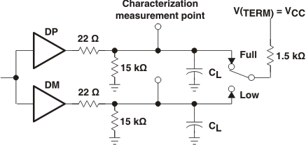
| tr | Transition rise time for DP or DM | See Figure 1 and Figure 2 | 4 | 20 | ns |
| tf | Transition fall time for DP or DM | See Figure 1 and Figure 2 | 4 | 20 | ns |
| t(RFM) | Rise/fall time matching(1) | (tr/tf) × 100 | 90% | 110% | |
| VO(CRS) | Signal crossover output voltage(1) | 1.3 | 2.0 | V | |
(1) Characterized only. Limits are approved by design and are not production tested.
7.7 Differential Driver Switching Characteristics (Low Speed Mode)
over recommended ranges of operating free-air temperature and supply voltage, CL = 50 pF (unless otherwise noted)| PARAMETER | TEST CONDITIONS | MIN | MAX | UNIT | ||
|---|---|---|---|---|---|---|
| tr | Transition rise time for DP or DM(1) | CL = 200 pF to 600 pF, See Figure 1 and Figure 2 | 75 | 300 | ns | |
| tf | Transition fall time for DP or DM(1) | CL = 200 pF to 600 pF, See Figure 1 and Figure 2 | 75 | 300 | ns | |
| t(RFM) | Rise/fall time matching(1) | (tr/tf) × 100 | 80% | 120% | ||
| VO(CRS) | Signal crossover output voltage(1) | CL = 200 pF to 600 pF | 1.3 | 2.0 | V | |
(1) Characterized only. Limits are approved by design and are not production tested.
 Figure 1. Differential Driver Switching Load
 Figure 2. Differential Driver Timing Waveforms
 Figure 3. Single-Ended Receiver Input Signal Parameter Definitions
7.8 Typical Characteristics
 Figure 4. Differential Receiver Input Sensitivity vs Common Mode Input Range