SLLSEO0D May 2015 – October 2017 TUSB211
PRODUCTION DATA.
- 1 Features
- 2 Applications
- 3 Description
- 4 Revision History
- 5 Pin Configuration and Functions
- 6 Specifications
- 7 Detailed Description
- 8 Application and Implementation
- 9 Power Supply Recommendations
- 10Layout
- 11Device and Documentation Support
- 12Mechanical, Packaging, and Orderable Information
Package Options
Mechanical Data (Package|Pins)
- RWB|12
Thermal pad, mechanical data (Package|Pins)
Orderable Information
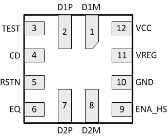
5 Pin Configuration and Functions
RWB Package
12 Pin (X2QFN)
Top View

Pin Functions
| PIN | I/O | INTERNAL PULLUP/PULLDOWN |
DESCRIPTION | |
|---|---|---|---|---|
| NAME | NO. | |||
| VCC | 12 | P | N/A | 3.3-V power |
| VREG | 11 | O | RSTN asserted: 30 kΩ PD | 1.8-V LDO output. Only enabled when operating in High Speed mode. Requires 0.1-µF external capacitor to GND to stabilize the core. |
| FS, LS mode: 30 kΩ PD | ||||
| HS mode: N/A | ||||
| GND | 10 | P | N/A | Ground |
| RSTN | 5 | I | 500 kΩ PU | Device disable/enable. Recommend 0.1-µF external capacitor to GND to ensure clean power on reset if not driven. |
| EQ | 6 | I | N/A | USB High Speed boost select via external pull down resistor. Sampled upon power up. Auto selects min EQ when left floating. Does not recognize real time adjustments. |
| D1P | 2 | I/O | N/A | USB High Speed positive port. Orientation independent – Can face either upstream or downstream. |
| D1M | 1 | I/O | N/A | USB High Speed negative port. Orientation independent – Can face either upstream or downstream. |
| D2P | 7 | I/O | N/A | USB High Speed positive port. Orientation independent – Can face either upstream or downstream. |
| D2M | 8 | I/O | N/A | USB High Speed negative port. Orientation independent – Can face either upstream or downstream. |
| TEST | 3 | I | RSTN asserted: 500 kΩ PD | No function. Leave floating. |
| ENA_HS | 9 | O | RSTN asserted: 500kΩ PD | Flag indicating that channel is in High Speed mode. Asserted upon:
De-asserted upon detection of disconnect or suspend. Can be left floating if not needed. |
| CD | 4 | O | RSTN asserted: 500 kΩ PD | Flag indicating that a USB device is attached. Asserted from an unconnected state upon detection of DP or DM pull-up resistor. De-asserted upon detection of disconnect. Can be left floating if not needed. |