SLLSEP2D August   2015  – May 2017 TUSB320HI , TUSB320LI

PRODUCTION DATA.  

  1. Features
  2. Applications
  3. Description
  4. Revision History
  5. Pin Configuration and Functions
  6. Specifications
    1. 6.1 Absolute Maximum Ratings
    2. 6.2 ESD Ratings
    3. 6.3 Recommended Operating Conditions
    4. 6.4 Thermal Information
    5. 6.5 Electrical Characteristics
    6. 6.6 Timing Requirements
    7. 6.7 Switching Characteristics
  7. Detailed Description
    1. 7.1 Overview
      1. 7.1.1 Cables, Adapters, and Direct Connect Devices
        1. 7.1.1.1 USB Type-C Receptacles and Plugs
        2. 7.1.1.2 USB Type-C Cables
        3. 7.1.1.3 Legacy Cables and Adapters
        4. 7.1.1.4 Direct Connect Devices
        5. 7.1.1.5 Audio Adapters
    2. 7.2 Feature Description
      1. 7.2.1 Port Role Configuration
        1. 7.2.1.1 Downstream Facing Port (DFP) - Source
        2. 7.2.1.2 Upstream Facing Port (UFP) - Sink
        3. 7.2.1.3 Dual Role Port (DRP)
      2. 7.2.2 Type-C Current Mode
      3. 7.2.3 Accessory Support
        1. 7.2.3.1 Audio Accessory
        2. 7.2.3.2 Debug Accessory
      4. 7.2.4 I2C and GPIO Control
      5. 7.2.5 VBUS Detection
    3. 7.3 Device Functional Modes
      1. 7.3.1 Unattached Mode
      2. 7.3.2 Active Mode
      3. 7.3.3 Dead Battery Mode
      4. 7.3.4 Shutdown Mode
    4. 7.4 Programming
    5. 7.5 Register Maps
      1. 7.5.1 CSR Registers (address = 0x00 - 0x07)
      2. 7.5.2 CSR Registers (address = 0x08)
      3. 7.5.3 CSR Registers (address = 0x09)
      4. 7.5.4 CSR Registers (address = 0x0A)
      5. 7.5.5 CSR Registers (address = 0x45)
      6. 7.5.6 CSR Registers (address = 0xA0)
  8. Application and Implementation
    1. 8.1 Application Information
    2. 8.2 Typical Application
      1. 8.2.1 DRP in I2C Mode
        1. 8.2.1.1 Design Requirements
        2. 8.2.1.2 Detailed Design Procedure
        3. 8.2.1.3 Application Curves
      2. 8.2.2 DFP in I2C Mode
        1. 8.2.2.1 Design Requirements
        2. 8.2.2.2 Detailed Design Procedure
        3. 8.2.2.3 Application Curves
      3. 8.2.3 UFP in I2C Mode
        1. 8.2.3.1 Design Requirements
        2. 8.2.3.2 Detailed Design Procedure
        3. 8.2.3.3 Application Curves
    3. 8.3 Initialization Set Up
      1. 8.3.1 TUSB320L Initialization Procedure
      2. 8.3.2 TUSB320H Initialization Procedure
  9. Power Supply Recommendations
  10. 10Layout
    1. 10.1 Layout Guidelines
    2. 10.2 Layout Example
  11. 11Device and Documentation Support
    1. 11.1 Related Links
    2. 11.2 Receiving Notification of Documentation Updates
    3. 11.3 Community Resources
    4. 11.4 Trademarks
    5. 11.5 Electrostatic Discharge Caution
    6. 11.6 Glossary
  12. 12Mechanical, Packaging, and Orderable Information

Package Options

Mechanical Data (Package|Pins)
Thermal pad, mechanical data (Package|Pins)
Orderable Information

Layout

Layout Guidelines

  1. An extra trace (or stub) is created when connecting between more than two points. A trace connecting pin A6 to pin B6 will create a stub because the trace also has to go to the USB Host. Ensure that:
    • A stub created by short on pin A6 (DP) and pin B6 (DP) at Type-C receptacle does not exceed 3.5 mm.
    • A stub created by short on pin A7 (DM) and pin B7 (DM) at Type-C receptacle does not exceed 3.5 mm.
  2. A 100-nF capacitor should be placed as close as possible to the TUSB320 VDD pin.

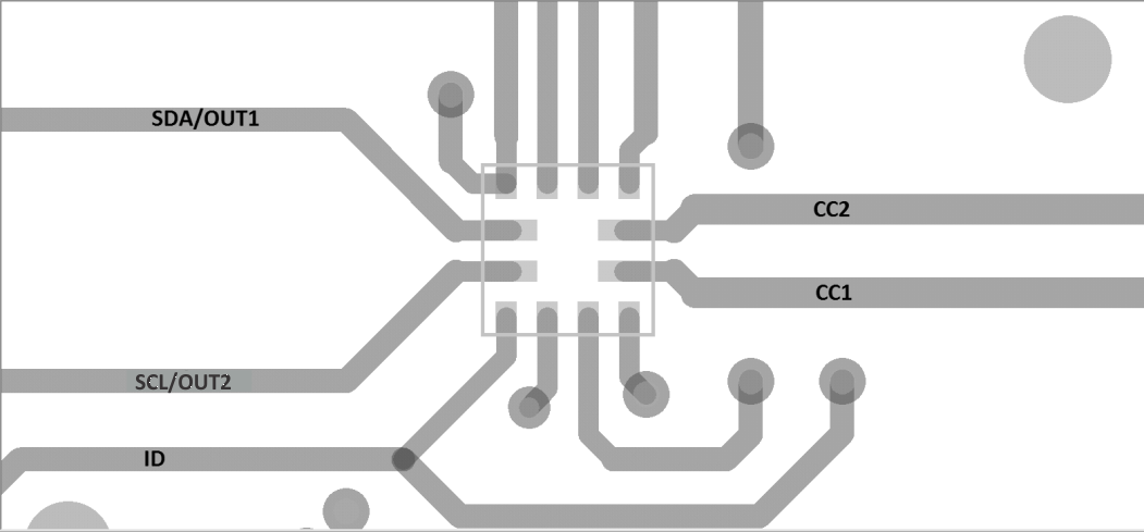
Layout Example

TUSB320HI TUSB320LI layout_sllsep2.gif Figure 22. TUSB320 Layout