SLLSEE6B July 2014 – January 2016 TUSB8041-Q1
PRODUCTION DATA.
- 1 Features
- 2 Applications
- 3 Description
- 4 Revision History
- 5 Description (Continued)
- 6 Pin Configuration and Functions
- 7 Specifications
-
8 Detailed Description
- 8.1 Overview
- 8.2 Functional Block Diagram
- 8.3 Feature Description
- 8.4 Device Functional Modes
- 8.5
Register Maps
- 8.5.1 Configuration Registers
- 8.5.2 ROM Signature Register
- 8.5.3 Vendor ID LSB Register
- 8.5.4 Vendor ID MSB Register
- 8.5.5 Product ID LSB Register
- 8.5.6 Product ID MSB Register
- 8.5.7 Device Configuration Register
- 8.5.8 Battery Charging Support Register
- 8.5.9 Device Removable Configuration Register
- 8.5.10 Port Used Configuration Register
- 8.5.11 Device Configuration Register 2
- 8.5.12 USB 2.0 Port Polarity Control Register
- 8.5.13 UUID Registers
- 8.5.14 Language ID LSB Register
- 8.5.15 Language ID MSB Register
- 8.5.16 Serial Number String Length Register
- 8.5.17 Manufacturer String Length Register
- 8.5.18 Product String Length Register
- 8.5.19 Serial Number String Registers
- 8.5.20 Manufacturer String Registers
- 8.5.21 Product String Registers
- 8.5.22 Additional Feature Configuration Register
- 8.5.23 Device Status and Command Register
-
9 Applications and Implementation
- 9.1 Application Information
- 9.2
Typical Application
- 9.2.1
Discrete USB Hub Product
- 9.2.1.1 Design Requirements
- 9.2.1.2
Detailed Design Procedure
- 9.2.1.2.1 Upstream Port Implementation
- 9.2.1.2.2 Downstream Port 1 Implementation
- 9.2.1.2.3 Downstream Port 2 Implementation
- 9.2.1.2.4 Downstream Port 3 Implementation
- 9.2.1.2.5 Downstream Port 4 Implementation
- 9.2.1.2.6 VBUS Power Switch Implementation
- 9.2.1.2.7 Clock, Reset, and Misc
- 9.2.1.2.8 TUSB8041-Q1 Power Implementation
- 9.2.1.3 Application Curves
- 9.2.1
Discrete USB Hub Product
- 10Power Supply Recommendations
- 11Layout
- 12Device and Documentation Support
- 13Mechanical, Packaging, and Orderable Information
Package Options
Refer to the PDF data sheet for device specific package drawings
Mechanical Data (Package|Pins)
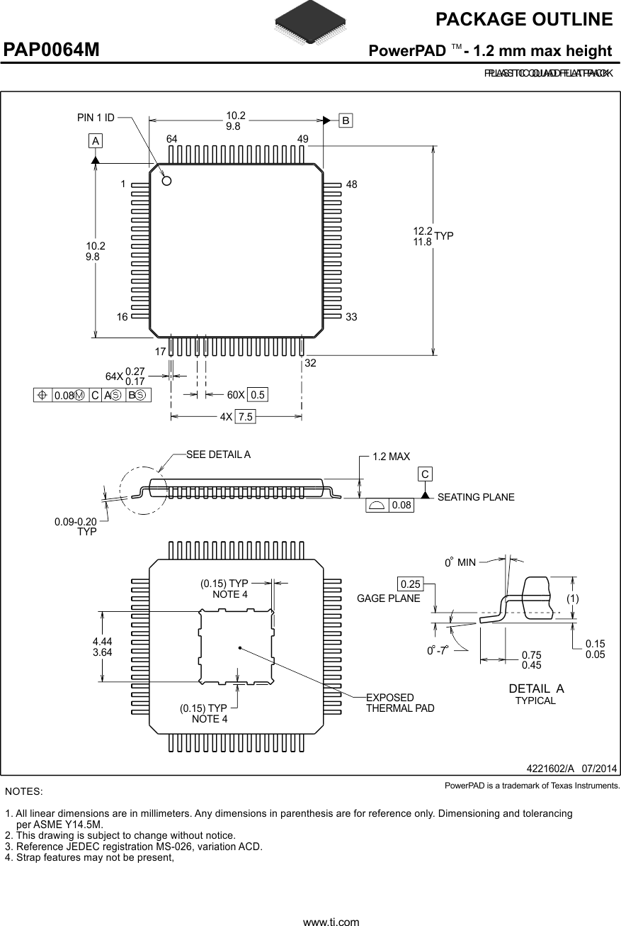
- PAP|64
Thermal pad, mechanical data (Package|Pins)
Orderable Information
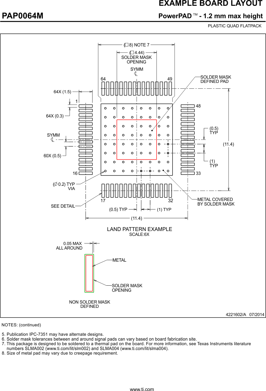
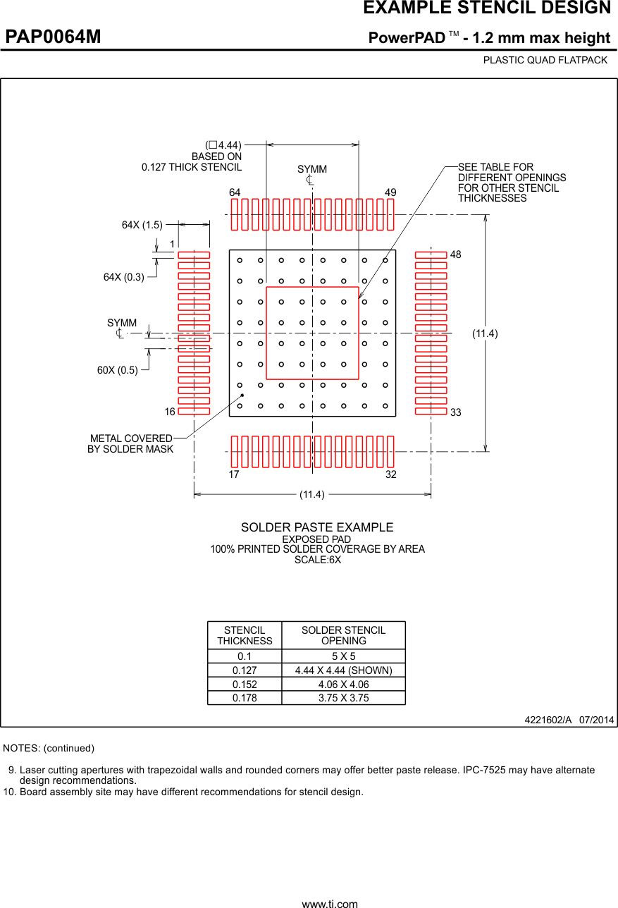
13 Mechanical, Packaging, and Orderable Information
The following pages include mechanical packaging and orderable information. This information is the most current data available for the designated devices. This data is subject to change without notice and revision of this document. For browser-based versions of this data sheet, refer to the left-hand navigation.


