SCES942A November 2021 – March 2022 TXU0202
PRODUCTION DATA
- 1 Features
- 2 Applications
- 3 Description
- 4 Revision History
- 5 Related Products
- 6 Pin Configuration and Functions—TXU0202
-
7 Specifications
- 7.1 Absolute Maximum Ratings
- 7.2 ESD Ratings
- 7.3 Recommended Operating Conditions
- 7.4 Thermal Information
- 7.5 Electrical Characteristics
- 7.6 Switching Characteristics, VCCA = 1.2 ± 0.1 V
- 7.7 Switching Characteristics, VCCA = 1.5 ± 0.1 V
- 7.8 Switching Characteristics, VCCA = 1.8 ± 0.15 V
- 7.9 Switching Characteristics, VCCA = 2.5 ± 0.2 V
- 7.10 Switching Characteristics, VCCA = 3.3 ± 0.3 V
- 7.11 Switching Characteristics, VCCA = 5.0 ± 0.5 V
- 7.12 Operating Characteristics
- 7.13 Typical Characteristics
- 8 Parameter Measurement Information
-
9 Detailed Description
- 9.1 Overview
- 9.2 Functional Block Diagram
- 9.3
Feature Description
- 9.3.1 CMOS Schmitt-Trigger Inputs with Integrated Pulldowns
- 9.3.2 Control Logic (OE) with VCC(MIN) Circuitry
- 9.3.3 Balanced High-Drive CMOS Push-Pull Outputs
- 9.3.4 VCC Isolation and VCC Disconnect
- 9.3.5 Over-Voltage Tolerant Inputs
- 9.3.6 Glitch-Free Power Supply Sequencing
- 9.3.7 Negative Clamping Diodes
- 9.3.8 Fully Configurable Dual-Rail Design
- 9.3.9 Supports High-Speed Translation
- 9.4 Device Functional Modes
- 10Application and Implementation
- 11Power Supply Recommendations
- 12Layout
- 13Device and Documentation Support
- 14Mechanical, Packaging, and Orderable Information
Package Options
Mechanical Data (Package|Pins)
Thermal pad, mechanical data (Package|Pins)
Orderable Information
5 Related Products
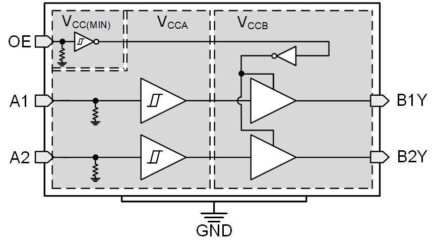
- TXU0x02 2-Bit Unidirectional Voltage-Level TranslatorsTXU0x02 are 2-bit, dual-supply noninverting fixed direction voltage level translators. These devices are compatible with the TXB0102 because of the same pinout, which allows for a drop in replacement. The OE pin can be referenced to either VCCA or VCCB logic levels allowing for one of the TXU0x02 devices to be used for fixed direction, high drive applications which the TXB0102 is not recommended to support.
- TXU0102TXU0102 is a 2-bit, dual-supply noninverting fixed direction voltage level translators with both channels in the same direction commonly used for GPIO translation.
 Figure 5-1 TXU0102 Functional Block Diagram