SLVS010X january   1976  – june 2023 UA78L

PRODUCTION DATA  

  1.   1
  2. Features
  3. Applications
  4. Description
  5. Revision History
  6. Pin Configuration and Functions
  7. Specifications
    1. 6.1  Absolute Maximum Ratings
    2. 6.2  ESD Ratings
    3. 6.3  Recommended Operating Conditions
    4. 6.4  Thermal Information
    5. 6.5  Electrical Characteristics: UA78L02 (Legacy Chip Only)
    6. 6.6  Electrical Characteristics: UA78L033 (New Chip Only)
    7. 6.7  Electrical Characteristics: UA78L05 (Both Legacy and New Chip)
    8. 6.8  Electrical Characteristics: UA78L12 (Both Legacy and New Chip)
    9. 6.9  Electrical Characteristics: UA78L06 (Legacy Chip Only)
    10. 6.10 Electrical Characteristics: UA78L08 (Legacy Chip Only)
    11. 6.11 Electrical Characteristics: UA78L09 (Legacy Chip Only)
    12. 6.12 Electrical Characteristics: UA78L10 (Legacy Chip Only)
    13. 6.13 Electrical Characteristics: UA78L15 (Both Legacy and New Chip)
    14. 6.14 Typical Characteristics
  8. Detailed Description
    1. 7.1 Overview
    2. 7.2 Functional Block Diagram
    3. 7.3 Feature Description
      1. 7.3.1 Current Limit
      2. 7.3.2 Thermal Shutdown
      3. 7.3.3 Dropout Voltage (VDO)
    4. 7.4 Device Functional Modes
      1. 7.4.1 Normal Operation
      2. 7.4.2 Dropout Operation
  9. Applications and Implementation
    1. 8.1 Application Information
    2. 8.2 Typical Application
      1. 8.2.1 Design Requirements
      2. 8.2.2 Detailed Design Procedure
        1. 8.2.2.1 Input and Output Capacitor Requirements
        2. 8.2.2.2 Power Dissipation (PD)
        3. 8.2.2.3 Estimating Junction Temperature
        4. 8.2.2.4 External Capacitor Requirements
        5. 8.2.2.5 Overload Recovery
        6. 8.2.2.6 Reverse Current
        7. 8.2.2.7 Polarity Reversal Protection
      3. 8.2.3 Application Curves
    3. 8.3 System Examples
      1. 8.3.1 Positive Regulator in Negative Configuration
      2. 8.3.2 Current Limiter Circuit
    4. 8.4 Power Supply Recommendations
    5. 8.5 Layout
      1. 8.5.1 Layout Guidelines
      2. 8.5.2 Layout Example
  10. Device and Documentation Support
    1. 9.1 Device Support
      1. 9.1.1 Development Support
        1. 9.1.1.1 Evaluation Module
      2. 9.1.2 Device Nomenclature
    2. 9.2 Receiving Notification of Documentation Updates
    3. 9.3 Support Resources
    4. 9.4 Trademarks
    5. 9.5 Electrostatic Discharge Caution
    6. 9.6 Glossary
  11. 10Mechanical, Packaging, and Orderable Information

Package Options

Refer to the PDF data sheet for device specific package drawings

Mechanical Data (Package|Pins)
  • D|8
  • PK|3
  • LP|3
Thermal pad, mechanical data (Package|Pins)
Orderable Information

Typical Characteristics

at specified junction temperature TJ = 25 °C, VI = 10 V, VO = 5 V, CIN = 0.33 µF, COUT = 0.1µF, and IO = 1 mA (unless otherwise noted)

GUID-20230207-SS0I-CHD6-0BFQ-Q0BLVRQZZSQP-low.svg
 
Figure 6-1 VO vs Temperature for New Chip
GUID-BD7A288E-3CFA-4DD0-9A0C-CB1AB55691C6-low.gif
 
Figure 6-3 Load Regulation for Legacy Chip
GUID-20230208-SS0I-MCFT-LDD4-WWPF5QW7T5DG-low.svg
 
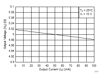
Figure 6-5 Load Regulation for New Chip
GUID-20230223-SS0I-85WR-HCLC-DRBTXT514NQL-low.svg
IO = 40 mA
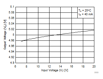
Figure 6-7 Line Regulation at IO = 40 mA for New Chip at TJ = 25°C
GUID-20230207-SS0I-905J-T0LM-CWNTKFDKTGCG-low.svg
IO = 40 mA
Figure 6-9 Line Regulation at IO = 40 mA for New Chip
GUID-25839AA3-168E-4D34-8A42-EC9C74A5E5D7-low.gif
 
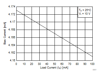
Figure 6-11 Bias Current vs Load Current for Legacy Chip
GUID-20230207-SS0I-CBKN-JFQJ-R7BQHFFGK6TV-low.svg
 
Figure 6-13 Bias Current vs Load Current for New Chip
GUID-20230223-SS0I-TCF8-XKFP-XGDLP4HMQZV5-low.svg
IO = 40 mA
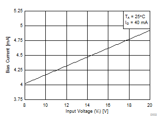
Figure 6-15 Bias Current vs Input Voltage for New Chip at TJ = 25°C
GUID-20230207-SS0I-KKBV-CMM4-RWG1GBTHDFH3-low.svg
 
Figure 6-17 Bias Current vs Input Voltage at IO = 1 mA for New Chip
GUID-20230207-SS0I-DJC8-Q50S-1X8ZNNQGX1S1-low.svg
VO = 90% of VO (typ)
Figure 6-19 ICL vs Temperature for New Chip
GUID-20230208-SS0I-2CTM-HF7K-3JXGFXJGF2P4-low.svg
VI = 23 V, VO = 15 V
Figure 6-21 Noise Spectral Density vs Frequency and IO for New Chip
GUID-20230208-SS0I-2HHV-NZFZ-CCSSWK4BFSFH-low.svg
VI = 23 V, VO = 15 V
Figure 6-23 PSRR vs Frequency and IO for New Chip
GUID-20230207-SS0I-PBVM-63JR-CJLN4Z7XHXGB-low.svg
IO = 40 mA
Figure 6-2 VO vs Temperature for New Chip
GUID-20230223-SS0I-69MD-QWKN-VN0PV0CJBCKK-low.svg
 
Figure 6-4 Load Regulation for New Chip at TJ = 25°C
GUID-130107B9-9C25-411A-97F3-A6AEA3A5926B-low.gif
IO = 40 mA
Figure 6-6 Line Regulation at IO = 40 mA for Legacy Chip
GUID-20230223-SS0I-2PVL-QS1F-01DPXG6FBL0Z-low.svg
 
Figure 6-8 Line Regulation at IO = 1 mA for New Chip at TJ = 25°C
GUID-20230207-SS0I-7LVK-DPH9-DLX56RRJDXVM-low.svg
 
Figure 6-10 Line Regulation at IO = 1 mA for New Chip
GUID-20230223-SS0I-XTKX-MQJB-BLDXZRBXBKRC-low.svg
 
Figure 6-12 Bias Current vs Load Current for New Chip at TJ = 25°C
GUID-09A9CA31-4166-4235-8E55-D130B125C463-low.gif
IO = 40 mA
Figure 6-14 Bias Current vs Input Voltage for Legacy Chip
GUID-20230207-SS0I-SLHQ-S2N4-6PVJW4GNXPL8-low.svg
IO = 40 mA
Figure 6-16 Bias Current vs Input Voltage for New Chip
GUID-20230207-SS0I-TPVJ-PBQJ-RQS1XMVDG6ZT-low.svg
VO = 0 V
Figure 6-18 ISC vs VI for New Chip
GUID-20230208-SS0I-PXK6-TK7T-7QJ912SR92RW-low.svg
VI = 9 V, VO = 3.3 V
Figure 6-20 Noise Spectral Density vs Frequency and IO for New Chip
GUID-20230208-SS0I-6CXW-MWGW-N45JVBPP1XJ4-low.svg
VI = 9 V, VO = 3.3 V
Figure 6-22 PSRR vs Frequency and IO for New Chip