SLUS872E January 2009 – February 2019 UC1842A-SP , UC1844A-SP
PRODUCTION DATA.
- 1 Features
- 2 Applications
- 3 Description
- 4 Revision History
- 5 Device Comparison Table
- 6 Pin Configuration and Functions
- 7 Specifications
- 8 Detailed Description
- 9 Application and Implementation
- 10Power Supply Recommendations
- 11Layout
- 12Device and Documentation Support
- 13Mechanical, Packaging, and Orderable Information
Package Options
Mechanical Data (Package|Pins)
- JG|8
Thermal pad, mechanical data (Package|Pins)
Orderable Information
9.2.2.2 Current Sensing and Limiting
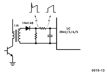
The UC184xA-SP current sense input is configured as shown in Figure 18. Current-to-voltage conversion is done externally with ground-referenced resistor RS. Under normal operation, the peak voltage across RS is controlled by the E/A according to the following relation:

where
- VC = Control voltage = E/A output voltage
RS can be connected to the power circuit directly or through a current transformer, as Figure 18 shows. While a direct connection is simpler, a transformer can reduce power dissipation in RS, reduce errors caused by the base current, and provide level shifting to eliminate the restraint of ground-referenced sensing. The relation between VC and peak current in the power stage is given by:

where
- N = Current sense transformer turns ratio = 1 when transformer not used.
For purposes of small-signal analysis, the control-to-sensed-current gain is:

When sensing current in series with the power transistor, as shown in Figure 18, the current waveform often has a large spike at its leading edge. This spike is due to rectifier recovery and/or inter-winding capacitance in the power transformer. If unattenuated, this transient can prematurely terminate the output pulse. As shown, a simple RC filter is usually adequate to suppress this spike. The RC time constant should be approximately equal to the current spike duration (usually a few hundred nanoseconds).
The inverting input to the UC184xA-SP current-sense comparator is internally clamped to 1 V (Figure 18). Current limiting occurs if the voltage at pin 3 reaches this threshold value, that is, the current limit is defined by:

 Figure 18. Transformer-Coupled Current Sensing