SLUSC14A May 2015 – February 2019 UC1845A-SP
PRODUCTION DATA.
- 1 Features
- 2 Applications
- 3 Description
- 4 Revision History
- 5 Device Comparison Table
- 6 Pin Configuration and Functions
- 7 Specifications
- 8 Detailed Description
- 9 Application and Implementation
- 10Power Supply Recommendations
- 11Layout
- 12Device and Documentation Support
- 13Mechanical, Packaging, and Orderable Information
Package Options
Refer to the PDF data sheet for device specific package drawings
Mechanical Data (Package|Pins)
- FK|20
- HKU|10
- JG|8
Thermal pad, mechanical data (Package|Pins)
Orderable Information
9.2.2.3 Error Amplifier
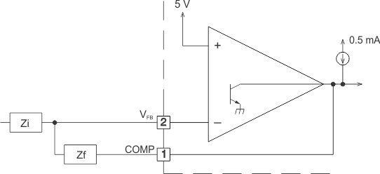
The error amplifier (E/A) configuration is shown in Figure 17. The non-inverting input is not brought out to a pin, but is internally biased to 5 V ±2%. The E/A output is available at pin 1 for external compensation, allowing the user to control the converter’s closed-loop frequency response.
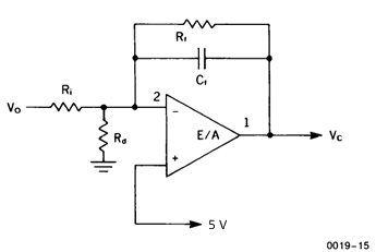
Figure 18 shows an E/A compensation circuit suitable for stabilizing any current-mode controlled topology except for flyback and boost converters operating with inductor current. The feedback components add a pole to the loop transfer function at ƒp = ½ π RF. RF and CF are chosen so that this pole cancels the zero of the output filter capacitor ESR in the power circuit. RI and RF fix the low-frequency gain. They are chosen to provide as much gain as possible while still allowing the pole formed by the output filter capacitor and load to roll off the loop gain to unity (0 dB) at ƒ ≈ ƒSWITCHING / 4. This technique ensures converter stability while providing good dynamic response.
 Figure 17. E/A Configuration
  Figure 18. Compensation
 The E/A output sources 0.5 mA and sinks 2 mA. A lower limit for RF is given by:

E/A input bias current (2-µA max) flows through RI, resulting in a DC error in output voltage (VO) given by:

Therefore, the designer should keep the value of RI, as low as possible.
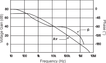
Figure 19 shows the open-loop frequency response of the UC1845A-SP E/A. The gain represents an upper limit on the gain of the compensated E/A. Phase lag increases rapidly as frequency exceeds 1 MHz due to second-order poles at about 10 MHz and above.
Continuous-inductor-current boost and flyback converters each have a right-half-plane zero in their transfer function. An additional compensation pole is needed to roll off loop gain at a frequency less than that of the RHP zero. RP and CP in the circuit of Figure 12 provide this pole.
 Figure 19. Error Amplifier Open-Loop Frequency Response