SLUS557G March 2003 – December 2016 UC28023 , UC28025
PRODUCTION DATA.
- 1 Features
- 2 Applications
- 3 Description
- 4 Revision History
- 5 Pin Configuration and Functions
- 6 Specifications
- 7 Parameter Measurement Information
- 8 Detailed Description
- 9 Application and Implementation
- 10Power Supply Recommendations
- 11Layout
- 12Device and Documentation Support
- 13Mechanical, Packaging, and Orderable Information
Package Options
Refer to the PDF data sheet for device specific package drawings
Mechanical Data (Package|Pins)
- DW|16
Thermal pad, mechanical data (Package|Pins)
Orderable Information
9 Application and Implementation
NOTE
Information in the following applications sections is not part of the TI component specification, and TI does not warrant its accuracy or completeness. TI’s customers are responsible for determining suitability of components for their purposes. Customers should validate and test their design implementation to confirm system functionality.
9.1 Application Information
The UC28023 and UC28025 are fixed-frequency PWM controllers optimized for high-frequency switched-mode power supply applications. The UC28023 is a single output PWM for single-ended topologies while the UC28025 offers dual alternating outputs for double-ended and full bridge topologies.
9.2 Typical Application
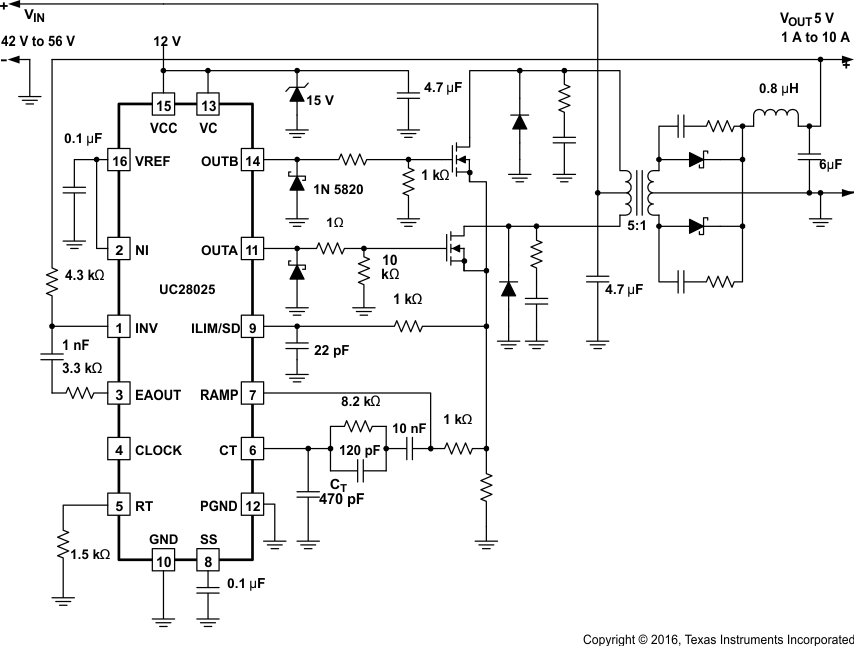
 Figure 18. DC-DC Push-Pull Converter Using UC28025
9.2.1 Design Requirements
For this design example, use the parameters listed in Table 1 as the input parameters.
Table 1. Design Parameters
| PARAMETER | EXAMPLE VALUE |
|---|---|
| Input voltage | 42 V to 56 V (48-V typical) |
| Output voltage | 5 V |
| Output current | 1 A to 10 A |
| Oscillator frequency | 1.5 MHz |
| Switching frequency | 750 kHz |
| Timing resistance | 1.5 kΩ |
| Timing capacitance | 470 pF |
9.2.2 Detailed Design Procedure
9.2.2.1 Timing Resistor and Capacitor Selection
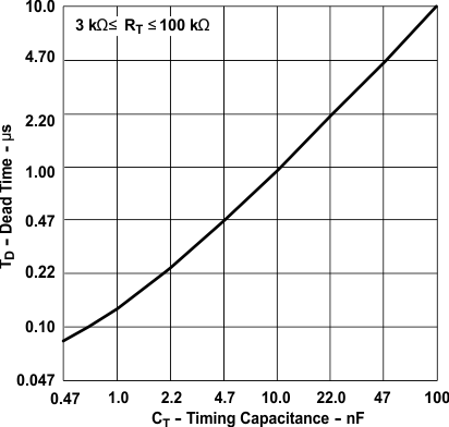
Generally, a higher switching frequency results in a smaller size but has higher switching losses. Operation at 750 kHz is used in this example as a reasonable compromise between size and efficiency. The values for timing resistance (RT) and timing capacitance (CT) are selected for the 1.5-MHz oscillator based on Figure 1.
9.2.2.2 Turns Ratio Selection
The maximum primary-to-secondary turns ratio (NMAX) can be determined with the target output voltage, minimum input voltage, and the estimated maximum duty cycle. DLIM = 0.35 is used for this example. NMAX can be calculated using Equation 1.

Rounding NMAX down to the next lowest integer results in a turns ratio of N = 5.
9.2.2.3 Inductor Selection
The maximum inductor ripple current occurs at the maximum input voltage. Typically, 20% to 40% of the full load current ripple is a good compromise between core loss and copper loss of the inductor. Higher ripple current allows for smaller inductor size, but places more burden on the output capacitor to smooth the ripple voltage on the output. In this example a ripple current of 25% of 10 A is used. The inductor value can be calculated with Equation 2.

The closest standard value of 0.8 µH is chosen for LO, this step is necessary if the chosen LO differs significantly from the value calculated in Equation 2. The actual ΔIL is based upon this selected inductor which must be calculated with Equation 3.

9.2.2.4 Rectifier Diode Selection
A rectifier diode must always possess low-forward voltage drop. When used in high-frequency switching applications, however, the diode must also posses a short recovery time. Schottky diodes meet both requirements and TI recommends their use for push-pull converter designs.
9.2.2.5 Snubber Components Selection
A resistor-capacitor snubber network crossing the low-side MOSFET reduces ringing and spikes at the switching node. Excessive ringing and spikes can cause erratic operation and may couple noise to the output voltage. Selecting the values for the snubber is best accomplished through empirical methods. First, make sure the lead lengths for the snubber connections are very short. Start with a resistor value between 5 Ω and 50 Ω. Increasing the value of the snubber capacitor results in more damping, but higher snubber losses. Select a minimum value for the snubber capacitor that provides adequate damping of the spikes on the switch node waveform at heavy load. A snubber may not be necessary with an optimized layout.
9.2.2.6 VCC and VC Capacitor Selection
The primary purpose of the VCC and VC capacitor is to supply the peak transient currents of the drivers as well as provide stability for the VCC and VC regulator. These peak currents can be several amperes. The value of the VCC and VC capacitor must at least 0.47 µF, and must be a good quality, low ESR, ceramic capacitor. The VCC and VC capacitor must be placed at the pins of the IC to minimize potentially damaging voltage transients caused by trace inductance. A value of 4.7 µF is used in this design.
9.2.2.7 Output Capacitor Selection
The output capacitors smooth the output voltage ripple caused by inductor ripple current and provide a source of charge during load transient conditions. In this design example, a 6-µF capacitor is selected as the main output capacitor.
9.2.2.8 Input Capacitor Selection
The input supply voltage typically has high source impedance at the switching frequency. Good quality input capacitors are necessary to limit the ripple voltage at the VIN pin while supplying most of the switch current during the on-time. The input capacitor must be selected for RMS current rating and minimum ripple voltage. In this example, a 4.7-µF capacitor is used. With ceramic capacitors, the input ripple voltage is triangular.
9.2.3 Application Curves
 Figure 19. Dead Time vs Timing Capacitance
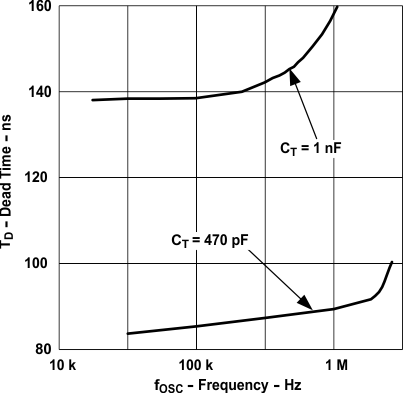
 Figure 20. Dead Time vs Frequency