SLUSCN0A November 2016 – January 2022 UCC20520
PRODUCTION DATA
- 1 Features
- 2 Applications
- 3 Description
- 4 Revision History
- 5 Pin Configuration and Functions
-
6 Specifications
- 6.1 Absolute Maximum Ratings
- 6.2 ESD Ratings
- 6.3 Recommended Operating Conditions
- 6.4 Thermal Information
- 6.5 Power Ratings
- 6.6 Insulation Specifications
- 6.7 Safety-Related Certifications
- 6.8 Safety-Limiting Values
- 6.9 Electrical Characteristics
- 6.10 Switching Characteristics
- 6.11 Insulation Characteristics Curves
- 6.12 Typical Characteristics
- 7 Parameter Measurement Information
- 8 Detailed Description
-
9 Application and Implementation
- 9.1 Application Information
- 9.2
Typical Application
- 9.2.1 Design Requirements
- 9.2.2
Detailed Design Procedure
- 9.2.2.1 Designing PWM Input Filter
- 9.2.2.2 Select External Bootstrap Diode and its Series Resistor
- 9.2.2.3 Gate Driver Output Resistor
- 9.2.2.4 Estimate Gate Driver Power Loss
- 9.2.2.5 Estimating Junction Temperature
- 9.2.2.6 Selecting VCCI, VDDA/B Capacitor
- 9.2.2.7 Dead Time Setting Guidelines
- 9.2.2.8 Application Circuits with Output Stage Negative Bias
- 9.2.2.9 56
- 9.2.3 Application Curves
- 10Layout
- 11Device and Documentation Support
Package Options
Mechanical Data (Package|Pins)
- DW|16
Thermal pad, mechanical data (Package|Pins)
- DW|16
Orderable Information
9.2.2.5 Estimating Junction Temperature
The junction temperature (TJ) of the UCC20520 can be estimated with:
Equation 18. 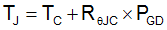
where
- TC is the UCC20520 case-top temperature measured with a thermocouple or some other instrument, RθJC is the Junction-to-case-top thermal resistance from the Section 6.4 table. Importantly, RθJA, the junction to ambient thermal impedance provided in the Thermal Information table, is developed based on JEDEC standard PCB board and it is subject to change when the PCB board layout is different.