SLUSA13E February 2010 – November 2023 UCC27321-Q1 , UCC27322-Q1
PRODUCTION DATA
- 1
- 1 Features
- 2 Applications
- 3 Description
- 4 Description (continued)
- 5 Related Products
- 6 Pin Configuration and Functions
- 7 Specifications
- 8 Detailed Description
- 9 Application and Implementation
- 10Power Supply Recommendations
- 11Layout
- 12Device and Documentation Support
- 13Revision History
- 14Mechanical, Packaging, and Orderable Information
Package Options
Mechanical Data (Package|Pins)
Thermal pad, mechanical data (Package|Pins)
- DGN|8
Orderable Information
3 Description
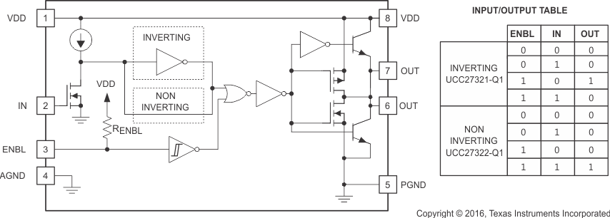
The UCC2732x-Q1 family of high-speed drivers delivers 9 A of peak drive current in an industry-standard pinout. These drivers can drive large MOSFETs for systems requiring extreme Miller current due to high dV/dt transitions. This eliminates additional external circuits and can replace multiple components to reduce space, design complexity, and assembly cost. Two standard logic options are offered, inverting (UCC27321-Q1) and noninverting (UCC27322-Q1).
Using a design that minimizes shoot-through current, the outputs of these devices can provide high gate drive current where it is most needed at the Miller plateau region during the MOSFET switching transition. A unique hybrid-output stage paralleling bipolar and MOSFET transistors (TrueDrive) allows efficient current delivery at low supply voltages. With this drive architecture, UCC2732x-Q1 can be used in industry standard 6-A, 9-A, and many 12-A driver applications. Latch-up and ESD protection circuits are also included. Finally, the UCC2732x-Q1 provides an enable (ENBL) function to better control the operation of the driver applications. ENBL is implemented on pin 3, which was previously left unused in the industry-standard pinout. It is internally pulled up to VDD for active-high logic and can be left open for standard operation.
| PART NUMBER | PACKAGE(1) | BODY SIZE (NOM) |
|---|---|---|
| UCC27321-Q1, UCC27322-Q1 | SOIC (8) | 6.00 mm × 4.90 mm |
| UCC27322-Q1 | MSOP-PowerPAD (8) | 4.90 mm × 3.00 mm |
 Functional Block Diagram