SLUSAW9F February 2012 – November 2014 UCC27511 , UCC27512
PRODUCTION DATA.
- 1 Features
- 2 Applications
- 3 Description
- 4 Revision History
- 5 Description (Continued)
- 6 UCC2751x Product Family
- 7 Pin Configuration and Functions
- 8 Specifications
- 9 Detailed Description
- 10Application and Implementation
- 11Power Supply Recommendations
- 12Layout
- 13Device and Documentation Support
- 14Mechanical, Packaging, and Orderable Information
Package Options
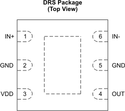
Mechanical Data (Package|Pins)
- DRS|6
Thermal pad, mechanical data (Package|Pins)
- DRS|6
Orderable Information
7 Pin Configuration and Functions
6-Pins
DBV Package
(Top View)
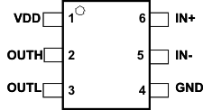
Pin Functions - UCC27511
| PIN | I/O | DESCRIPTION | |
|---|---|---|---|
| NO. | NAME | ||
| 1 | VDD | I | Bias supply input. |
| 2 | OUTH | O | Sourcing current output of driver. Connect resistor between OUTH and Gate of power-switching device to adjust turnon speed. |
| 3 | OUTL | O | Sinking current output of driver. Connect resistor between OUTL and Gate of power-switching device to adjust turnoff speed. |
| 4 | GND | - | Ground: All signals referenced to this pin. |
| 5 | IN- | I | Inverting input: When the driver is used in noninverting configuration, connect IN- to GND in order to enable output, OUT held LOW if IN- is unbiased or floating |
| 6 | IN+ | I | Noninverting input: When the driver is used in inverting configuration, connect IN+ to VDD in order to enable output, OUT held LOW if IN+ is unbiased or floating |
Pin Functions - UCC27512
| PIN | I/O | DESCRIPTION | |
|---|---|---|---|
| NO. | NAME | ||
| 1 | IN+ | I | Noninverting input: When the driver is used in inverting configuration, connect IN+ to VDD in order to enable output, OUT held LOW if IN+ is unbiased or floating. |
| 2, 5 | GND | - | Ground: All signals referenced to this pin. TI recommends to connect pin 2 and pin 5 on PCB as close to the device as possible. |
| 3 | VDD | I | Bias supply input. |
| 4 | OUT | O | Sourcing/sinking current output of driver. |
| 6 | IN- | I | Inverting input: When the driver is used in noninverting configuration, connect IN- to GND in order to enable output, OUT held LOW if IN- is unbiased or floating. |