SLUSFL4A April   2024  – October 2024 UCC27614-Q1

PRODUCTION DATA  

  1.   1
  2. Features
  3. Applications
  4. Description
  5. Pin Configuration and Functions
  6. Specifications
    1. 5.1 Absolute Maximum Ratings
    2. 5.2 ESD Ratings
    3. 5.3 Recommended Operating Conditions
    4. 5.4 Thermal Information
    5. 5.5 Electrical Characteristics
    6. 5.6 Switching Characteristics
    7. 5.7 Timing Diagrams
    8. 5.8 Typical Characteristics
  7. Detailed Description
    1. 6.1 Overview
    2. 6.2 Functional Block Diagram
    3. 6.3 Feature Description
      1. 6.3.1 VDD Undervoltage Lockout
      2. 6.3.2 Input Stage
      3. 6.3.3 Enable Function
      4. 6.3.4 Output Stage
    4. 6.4 Device Functional Modes
  8. Applications and Implementation
    1. 7.1 Application Information
    2. 7.2 Typical Application
      1. 7.2.1 Driving MOSFET/IGBT/SiC MOSFET
        1. 7.2.1.1 Design Requirements
        2. 7.2.1.2 Detailed Design Procedure
          1. 7.2.1.2.1 Input-to-Output Configuration
          2. 7.2.1.2.2 Input Threshold Type
          3. 7.2.1.2.3 VDD Bias Supply Voltage
          4. 7.2.1.2.4 Peak Source and Sink Currents
          5. 7.2.1.2.5 Enable and Disable Function
          6. 7.2.1.2.6 Propagation Delay and Minimum Input Pulse Width
          7. 7.2.1.2.7 Power Dissipation
        3. 7.2.1.3 Application Curves
  9. Power Supply Recommendations
  10. Layout
    1. 9.1 Layout Guidelines
    2. 9.2 Layout Example
    3. 9.3 Thermal Consideration
  11. 10Device and Documentation Support
    1. 10.1 Third-Party Products Disclaimer
    2. 10.2 Receiving Notification of Documentation Updates
    3. 10.3 Support Resources
    4. 10.4 Trademarks
    5. 10.5 Electrostatic Discharge Caution
    6. 10.6 Glossary
  12. 11Revision History
  13. 12Mechanical, Packaging, and Orderable Information

Package Options

Refer to the PDF data sheet for device specific package drawings

Mechanical Data (Package|Pins)
  • D|8
  • DGN|8
  • DSG|8
Thermal pad, mechanical data (Package|Pins)
Orderable Information

Typical Characteristics

Unless otherwise specified, VDD = 12 V, IN+ = 3.3 V, IN- = GND, TJ = 25 °C, No load

UCC27614-Q1 Peak
                        Source Current vs VDDFigure 5-4 Peak Source Current vs VDD
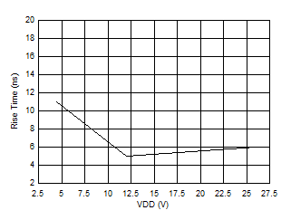
UCC27614-Q1 Output Rise Time vs VDD
CLOAD = 1.8 nF
Figure 5-6 Output Rise Time vs VDD
UCC27614-Q1 Output Rise and Fall Time vs
                        Temperature
CLOAD = 1.8 nF
Figure 5-8 Output Rise and Fall Time vs Temperature
UCC27614-Q1 Falling (Turnoff) Propagation Delay vs VDD
CLOAD = 1.8 nF
Figure 5-10 Falling (Turnoff) Propagation Delay vs VDD
UCC27614-Q1 Operating Supply Current vs VDDFigure 5-12 Operating Supply Current vs VDD
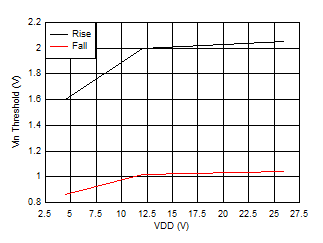
UCC27614-Q1 Input
                        Threshold vs VDDFigure 5-14 Input Threshold vs VDD
UCC27614-Q1 Input Threshold Hysteresis vs Temperature Figure 5-16 Input Threshold Hysteresis vs Temperature
UCC27614-Q1 Output Pullup Resistance vs
                        TemperatureFigure 5-18 Output Pullup Resistance vs Temperature
UCC27614-Q1 Output Pulldown Resistance vs
                        TemperatureFigure 5-20 Output Pulldown Resistance vs Temperature
UCC27614-Q1 UVLO Hysteresis vs Temperature Figure 5-22 UVLO Hysteresis vs Temperature
UCC27614-Q1 Peak
                        Sink Current vs VDDFigure 5-5 Peak Sink Current vs VDD
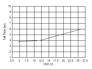
UCC27614-Q1 Output Fall Time vs VDD
CLOAD = 1.8 nF
Figure 5-7 Output Fall Time vs VDD
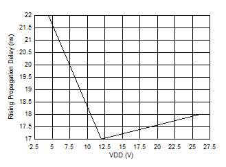
UCC27614-Q1 Rising (Turnon) Propagation Delay vs VDD
CLOAD = 1.8 nF
Figure 5-9 Rising (Turnon) Propagation Delay vs VDD
UCC27614-Q1 Propagation Delay vs
                        Temperature
CLOAD = 1.8 nF
Figure 5-11 Propagation Delay vs Temperature
UCC27614-Q1 Operating Static Supply Current vs TemperatureFigure 5-13 Operating Static Supply Current vs Temperature
UCC27614-Q1 Input Threshold vs Temperature Figure 5-15 Input Threshold vs Temperature
UCC27614-Q1 Output Pullup Resistance vs VDDFigure 5-17 Output Pullup Resistance vs VDD
UCC27614-Q1 Output Pulldown Resistance vs VDDFigure 5-19 Output Pulldown Resistance vs VDD
UCC27614-Q1 UVLO Threshold vs
                        Temperature Figure 5-21 UVLO Threshold vs Temperature