SLUS828D December 2008 – October 2017 UCC28019A
PRODUCTION DATA.
- 1 Features
- 2 Applications
- 3 Description
- 4 Revision History
- 5 Pin Configuration and Functions
- 6 Specifications
-
7 Detailed Description
- 7.1 Overview
- 7.2 Functional Block Diagram
- 7.3
Feature Description
- 7.3.1 Soft-Start
- 7.3.2
System Protection
- 7.3.2.1 VCC Undervoltage Lockout (UVLO)
- 7.3.2.2 Input Brown-Out Protection (IBOP)
- 7.3.2.3 Output Overvoltage Protection (OVP)
- 7.3.2.4 Open Loop Protection/Standby (OLP/Standby)
- 7.3.2.5 ISENSE Open-Pin Protection (ISOP)
- 7.3.2.6 Output Undervoltage Detection (UVD) and Enhanced Dynamic Response (EDR)
- 7.3.2.7 Over-Current Protection
- 7.3.2.8 Soft Over Current (SOC)
- 7.3.2.9 Peak Current Limit (PCL)
- 7.3.2.10 Current Sense Resistor, RISENSE
- 7.3.3 Gate Driver
- 7.3.4 Current Loop
- 7.3.5 ISENSE and ICOMP Functions
- 7.3.6 Pulse Width Modulator
- 7.3.7 Control Logic
- 7.3.8 Voltage Loop
- 7.3.9 Output Sensing
- 7.3.10 Voltage Error Amplifier
- 7.3.11 Non-Linear Gain Generation
- 7.4 Device Functional Modes
- 8 Application and Implementation
- 9 Power Supply Recommendations
- 10Layout
- 11Device and Documentation Support
- 12Mechanical, Packaging, and Orderable Information
Package Options
Mechanical Data (Package|Pins)
- D|8
Thermal pad, mechanical data (Package|Pins)
Orderable Information
8 Application and Implementation
NOTE
Information in the following applications sections is not part of the TI component specification, and TI does not warrant its accuracy or completeness. TI’s customers are responsible for determining suitability of components for their purposes. Customers should validate and test their design implementation to confirm system functionality.
8.1 Application Information
The UCC28019A is a switch-mode controller used in boost converters for power factor correction operating at a fixed frequency in continuous conduction mode. The UCC28019A requires few external components to operate as an active PFC pre-regulator. The operating switching frequency is fixed at 65 kHz.
The internal 5-V reference voltage provides for accurate output voltage regulation over the typical world-wide 85-VAC to 265-VAC mains input range from zero to full output load. The usable system load ranges from 100 W to few kW.
Regulation is accomplished in two loops. The inner current loop shapes the average input current to match the sinusoidal input voltage under continuous inductor current conditions. Under light-load conditions, depending on the boost inductor value, the inductor current may go discontinuous but still meet Class-A/D requirements of IEC 61000-3-2 despite the higher harmonics. The outer voltage loop regulates the PFC output voltage by generating a voltage on VCOMP (dependent upon the line and load conditions) which determines the internal gain parameters for maintaining a low-distortion, steady-state, input-current wave shape.
8.2 Typical Application
Figure 26 illustrates the design process and component selection for a continuous conduction mode power factor correction boost converter utilizing the UCC28019A. The target design is a universal input, 350-W PFC designed for an ATX supply application. This design process is directly tied to the UCC28019A Design Calculator (SLUC117) spreadsheet that can be found in the Tools section of the UCC28019A product folder on the Texas Instruments website.
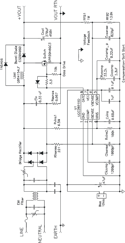 Figure 26. Design Example Schematic
8.2.1 Design Requirements
Design goal parameters for a continuous conduction mode power factor correction boost converter utilizing the UCC28019A.
Table 1. Design Goal Parameters
| PARAMETER | TEST CONDITION | MIN | TYP | MAX | UNIT | |
|---|---|---|---|---|---|---|
| Input characteristics | ||||||
| VIN | Input voltage | 85 | 115 | 265 | VAC | |
| fLINE | Input frequency | 47 | 63 | Hz | ||
| Brown out voltage | VAC(on), IOUT = 0.9 A | 75 | VAC | |||
| VAC(off), IOUT = 0.9 A | 65 | VAC | ||||
| Output characteristics | ||||||
| VOUT | Output voltage | 85 VAC ≤ VIN ≤ 265 VAC, 47 Hz ≤ fLINE ≤ 63 Hz 0 A ≤ IOUT ≤ 0.9 A |
380 | 390 | 402 | VDC |
| VRIPPLE(SW) | High frequency output voltage ripple | VIN = 115 VAC, fLINE = 60 Hz, IOUT = 0.9 A | 3.9 | VPP | ||
| VIN = 230 VAC , fLINE = 50 Hz, IOUT = 0.9 A | 3.9 | VPP | ||||
| VRIPPLE(f_LINE) | Line frequency output voltage ripple | VIN = 115 VAC, fLINE = 60 Hz, IOUT = 0.9 A | 19.5 | VPP | ||
| VIN = 230 VAC, fLINE = 50 Hz, IOUT = 0.9 A | 19.5 | VPP | ||||
| IOUT | Output load current | 85 VAC ≤ VIN ≤ 265 VAC, 47 Hz ≤ fLINE ≤ 63 Hz | 0.9 | A | ||
| POUT | Output power | 350 | W | |||
| VOUT(OVP) | Output over voltage protection | 410 | V | |||
| VOUT(UVP) | Output under voltage protection | 370 | V | |||
| Control loop characteristics | ||||||
| fSW | Switching frequency | TJ = 25°C | 61.7 | 65 | 68.3 | kHz |
| f(CO) | Control loop bandwidth | VIN = 162 VDC, IOUT = 0.45 A | 14 | Hz | ||
| Phase margin | VIN = 162 VDC, IOUT = 0.45 A | 70 | degrees | |||
| PF | Power factor | VIN = 115 VAC, IOUT = 0.9 A | 0.98 | |||
| THD | Total harmonic distortion | VIN = 115 VAC, fLINE = 60 Hz, IOUT = 0.9 A | 4.3% | 10% | ||
| VIN = 230 VAC, fLINE = 50 Hz, IOUT = 0.9 A | 6.6% | 10% | ||||
| η | Full load efficiency | VIN = 115 VAC, fLINE = 60 Hz, IOUT = 0.9 A | 0.95 | |||
| TAMB | Ambient temperature | 50 | °C | |||
8.2.2 Detailed Design Procedure
8.2.2.1 Current Calculations
First, determine the maximum average output current, IOUT(max):


The maximum input RMS line current, IIN_RMS(max), is calculated using the parameters from Table 1 and the efficiency and power factor initial assumptions:


Based upon the calculated RMS value, the maximum peak input current, IIN_PEAK(max), and the maximum average input current, IIN_AVG(max), assuming the waveform is sinusoidal, can be determined.


8.2.2.2 Bridge Rectifier
Assuming a forward voltage drop, VF_BRIDGE, of 0.95 V across the rectifier diodes, BR1, the power loss in the input bridge, PBRIDGE, can be calculated:


8.2.2.3 Input Capacitor
Note that the UCC28019A is a continuous conduction mode controller and as such the inductor ripple current should be sized accordingly. High inductor ripple current has an impact on the CCM/DCM boundary and results in higher light-load THD, and also affects the choices for RSENSE and CICOMP values. Allowing an inductor ripple current, IRIPPLE, of 20% and a high frequency ripple voltage factor, ΔVRIPPLE_IN, of 6%, the minimum input capacitor value, CIN, is calculated by first determining the input ripple current, IRIPPLE, and the input ripple voltage, VIN_RIPPLE(max):


The value for the input x-capacitor can now be calculated:


A 0.33 μF, 275 VAC ex-2 film capacitor was selected for CIN.
8.2.2.4 Boost Inductor
The boost inductor, LBST, is selected after determining the maximum inductor peak current, IL_PEAK(max):


The minimum value of the boost inductor is calculated based upon a worst case duty cycle of 0.5:


The actual value of the boost inductor that will be used is 1.25 mH.
The maximum duty cycle, DUTY(max), can be calculated and will occur at the minimum input voltage:


8.2.2.5 Boost Diode
The diode losses are estimated based upon the forward voltage drop, VF, at 125°C and the reverse recovery charge, QRR, of the diode. This design uses a silicon-carbide diode. Although somewhat more expensive, it essentially eliminates the reverse recovery losses because QRR is equal to 0nC.


8.2.2.6 Switching Element
The conduction losses of the switch are estimated using the RDS(on) of the FET at 125°C , found in the FET data sheet, and the calculated drain to source RMS current, IDS_RMS:


The switching losses are estimated using the rise time, (tr), and fall time, (tf), of the gate, and the output capacitance losses.
For the selected device:


Total FET losses:

8.2.2.7 Sense Resistor
To accommodate the gain of the internal non-linear power limit, RSENSE is sized such that it will trigger the soft over-current at 25% higher than the maximum peak inductor current using the minimum SOC threshold, VSOC, of ISENSE.


Using a parallel combination of available standard value resistors, the sense resistor is chosen.

The power dissipated across the sense resistor, PRsense, must be calculated:


The peak current limit, PCL, protection feature will be triggered when current through the sense resistor results in the voltage across RSENSE to be equal to the VPCL threshold. For a worst case analysis, the maximum VPCL threshold is used:


To protect the device from inrush current, a standard 220-Ω resistor, RISENSE, is placed in series with the ISENSE pin. A 1000-pF capacitor, CISENSE, is placed close to the device to improve noise immunity on the ISENSE pin.
8.2.2.8 Output Capacitor
The output capacitor, COUT, is sized to meet holdup requirements of the converter. Assuming the downstream converters require the output of the PFC stage to never fall below 300 V, VOUT_HOLDUP(min), during one line cycle, tHOLDUP = 1/fLINE(min), the minimum calculated value for the capacitor is:


It is advisable to de-rate this capacitor value by 20%; the actual capacitor used is 270 μF.
Setting the maximum peak-to-peak output ripple voltage to be less than 5% of the output voltage will ensure that the ripple voltage will not trigger the output over-voltage or output under-voltage protection features of the controller. The maximum peak-to-peak ripple voltage, occurring at twice the line frequency, and the ripple current of the output capacitor are calculated:


The required ripple current rating at twice the line frequency is equal to:


There will also be a high frequency ripple current through the output capacitor:


The total ripple current in the output capacitor is the combination of both and the output capacitor must be selected accordingly:


8.2.2.9 Output Voltage Set Point
For low power dissipation and minimal contribution to the voltage set point error, it is recommended to use 1 MΩ for the top voltage feedback divider resistor, RFB1. Multiple resistors in series are used due to the maximum allowable voltage across each. Using the internal 5-V reference, VREF, select the bottom divider resistor, RFB2, to meet the output voltage design goals.


Using 13 kΩ for RFB2 results in a nominal output voltage set point of 391 V.
The over-voltage protection, OVD, will be triggered when the output voltage exceeds 5% of its nominal set-point:


The under-voltage detection, UVD, will be triggered when the output voltage falls below 5% of its nominal set-point:


A small capacitor on VSENSE must be added to filter out noise. Limit the value of the filter capacitor such that the RC time constant is less than 0.1 ms so as not to significantly reduce the control response time to output voltage deviations. With careful layout, the noise on this design is minimal, so an RC time constant of 0.01 ms was all that was needed:


8.2.2.10 Loop Compensation
The selection of compensation components, for both the current loop and the voltage loop, is made easier by using the UCC28019A Design Calculator spreadsheet that can be found in the Tools section of the UCC28019A product folder on the Texas Instruments website. The current loop is compensated first by determining the product of the internal loop variables, M1M2, using the internal controller constants K1 and KFQ:


The VCOMP operating point is found on Figure 27. The Design Calculator spreadsheet enables the user to iteratively select the appropriate VCOMP value.
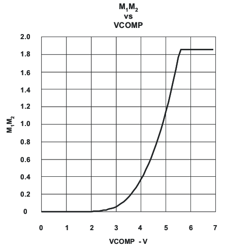 Figure 27. M1M2 vs. VCOMP
For the given M1M2 of 0.374 V/μs, the VCOMP is approximately equal to 4, as shown in Figure 27.
The individual loop factors, M1 which is the current loop gain factor, and M2 which is the voltage loop PWM ramp slope, are calculated using the following conditions:
The M1 current loop gain factor:
- if : 0 < VCOMP < 2

- if : 2 ≤ VCOMP < 3

- if : 3 ≤ VCOMP < 5.5

- if : 5.5 ≤ VCOMP < 7

In this example:

The M2 PWM ramp slope:
- if : 0 < VCOMP < 1.5

- if : 1.5 ≤ VCOMP < 5.6

- if : 5.6 ≤ VCOMP < 7

In this example:

Verify that the product of the individual gain factors is approximately equal to the M1M2 factor determined above, if not, reselect VCOMP and recalculate M1M2.


The non-linear gain variable, M3, can now be calculated:
- if : 0 < VCOMP < 3

- if : 3 ≤ VCOMP < 7

In this example:

The frequency of the current averaging pole, fIAVG, is chosen to be at 9.5 kHz. The required capacitor on ICOMP, CICOMP, for this is determined using the transconductance gain, gmi, of the internal current amplifier:


Using a 1200 pF capacitor for CICOMP results in a current averaging pole frequency of 8.7 kHz:


The transfer function of the current loop can be plotted:


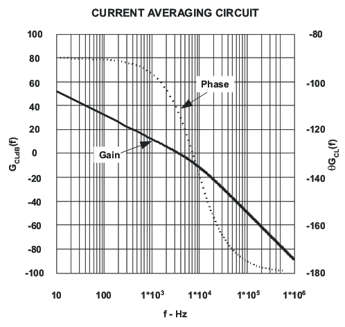 Figure 28. Bode Plot of the Current Averaging Circuit.
The open loop of the voltage transfer function, GVL(f) contains the product of the voltage feedback gain, GFB, and the gain from the pulse width modulator to the power stage, GPWM_PS, which includes the pulse width modulator to power stage pole, fPWM_PS. The plotted result is shown in Figure 29.


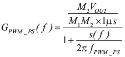


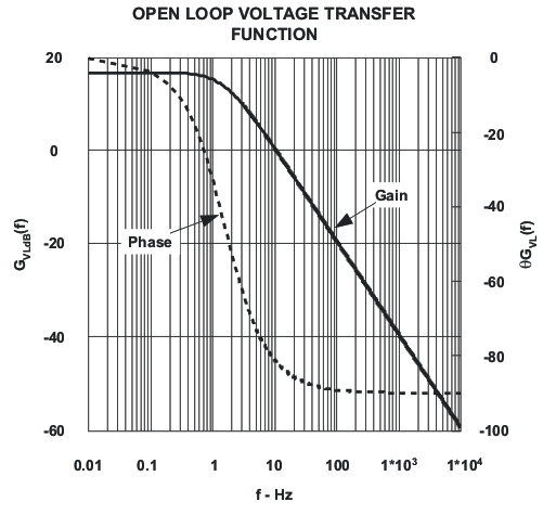 Figure 29. Bode Plot of the Open Loop Voltage Transfer Function
The voltage error amplifier is compensated with a zero, fZERO, at the fPWM_PS pole and a pole, fPOLE, placed at 20 Hz to reject high frequency noise and roll off the gain amplitude. The overall voltage loop crossover, fV, is desired to be at 10 Hz. The compensation components of the voltage error amplifier are selected accordingly.


From Figure 29, and the Design Calculator spreadsheet, the open loop gain of the voltage transfer function at 10 Hz is approximately 0.667 dB. Estimating that the parallel capacitor, CVCOMP_P, is much smaller than the series capacitor, CVCOMP, the unity gain will be at fV, and the zero will be at fPWM_PS, the series compensation capacitor is determined:


A 3.3-μF capacitor is used for CVCOMP.


A 33.2-kΩ resistor is used for RVCOMP.


A 0.22-μF capacitor is used for CVCOMP_P.
The total closed loop transfer function, GVL_total, contains the combined stages and is plotted in Figure 30.


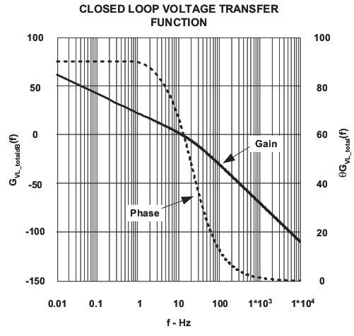 Figure 30. Closed Loop Voltage Bode Plot
8.2.2.11 Brown Out Protection
Select the top divider resistor into the VINS pin so as not to contribute excessive power loss. The extremely low bias current into VINS means the value of RVINS1 could be hundreds of megaOhms. For practical purposes, a value less than 10 MΩ is usually chosen. Assuming approximately 150 times the input bias current through the resistor dividers will result in an RVINS1 that is less than 10 MΩ , so as to not contribute excessive noise, and still maintain minimal power loss. The brown out protection will turn off the gate drive when the input falls below the user programmable minimum voltage, VAC(off), and turn on when the input rises above VAC(on).


A 6.5-M resistance is chosen.


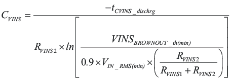
The capacitor on VINS, CVINS, is selected so that it's discharge time is greater than the output capacitor hold up time. COUT was chosen to meet one-cycle hold-up time so CVINS will be chosen to meet 2.5 half-line cycles.



8.2.3 Application Curves
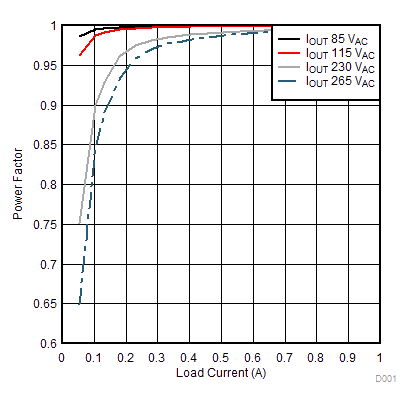 Figure 31. Power Factor vs. Load Current
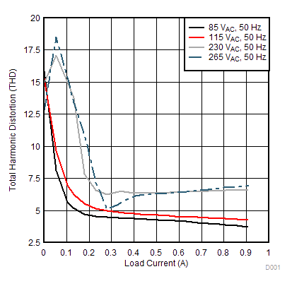 Figure 32. Total Harmonic Distortion vs. Load Current