SGLS121D December 2002 – June 2020 UCC2800-Q1 , UCC2801-Q1 , UCC2802-Q1 , UCC2803-Q1 , UCC2804-Q1 , UCC2805-Q1
PRODUCTION DATA.
- 1 Features
- 2 Applications
- 3 Description
- 4 Revision History
- 5 Description (continued)
- 6 Device Comparison Table
- 7 Pin Configuration and Functions
- 8 Specifications
-
9 Detailed Description
- 9.1 Overview
- 9.2 Functional Block Diagram
- 9.3
Feature Description
- 9.3.1 Detailed Pin Description
- 9.3.2 Undervoltage Lockout (UVLO)
- 9.3.3 Self-Biasing, Active Low Output
- 9.3.4 Reference Voltage
- 9.3.5 Oscillator
- 9.3.6 Synchronization
- 9.3.7 PWM Generator
- 9.3.8 Minimum Off-Time Setting (Dead-Time Control)
- 9.3.9 Leading Edge Blanking
- 9.3.10 Minimum Pulse Width
- 9.3.11 Current Limiting
- 9.3.12 Overcurrent Protection and Full Cycle Restart
- 9.3.13 Soft Start
- 9.3.14 Slope Compensation
- 9.4 Device Functional Modes
- 10Application and Implementation
- 11Power Supply Recommendations
- 12Layout
- 13Device and Documentation Support
- 14Mechanical, Packaging, and Orderable Information
Package Options
Refer to the PDF data sheet for device specific package drawings
Mechanical Data (Package|Pins)
- D|8
Thermal pad, mechanical data (Package|Pins)
Orderable Information
10.2.3 Application Curves
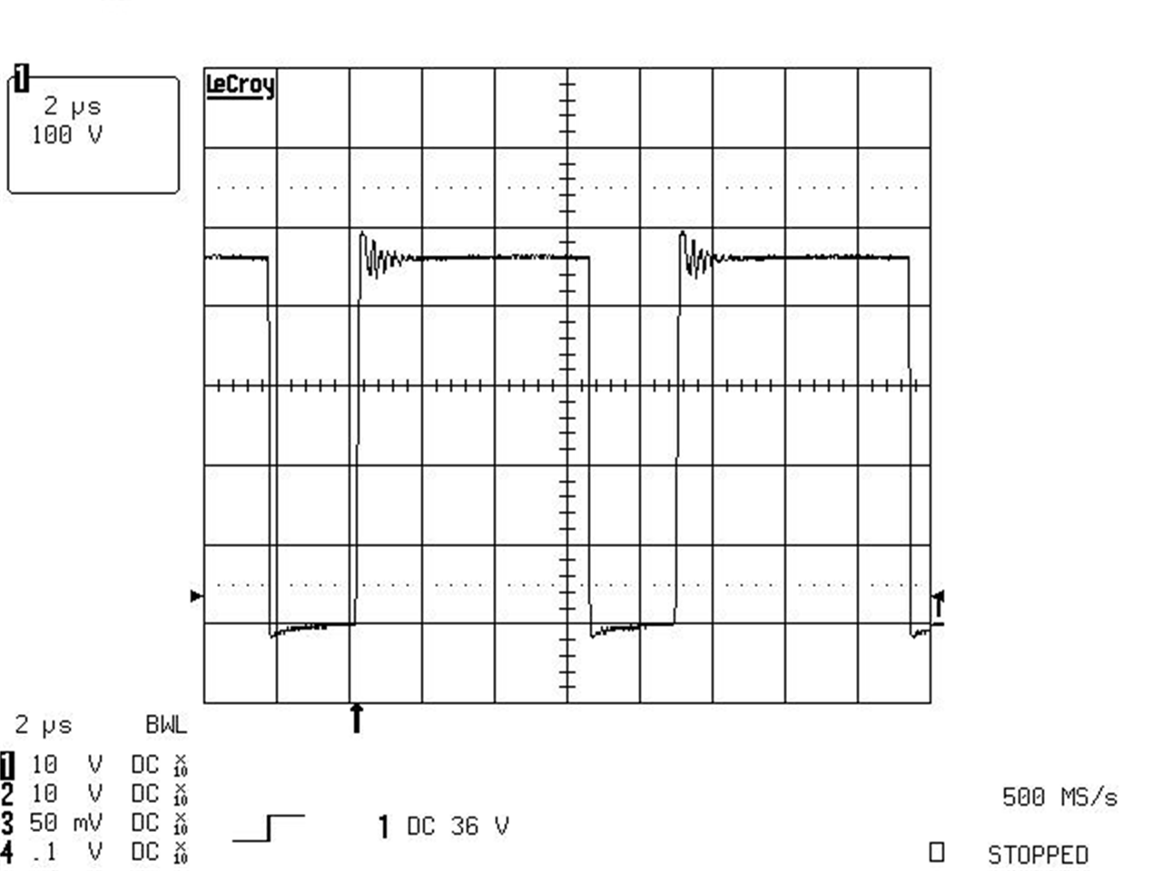 Figure 38. Primary Side MOSFET Drain to Source Voltage at 240-V AC Input (100 V/div)
 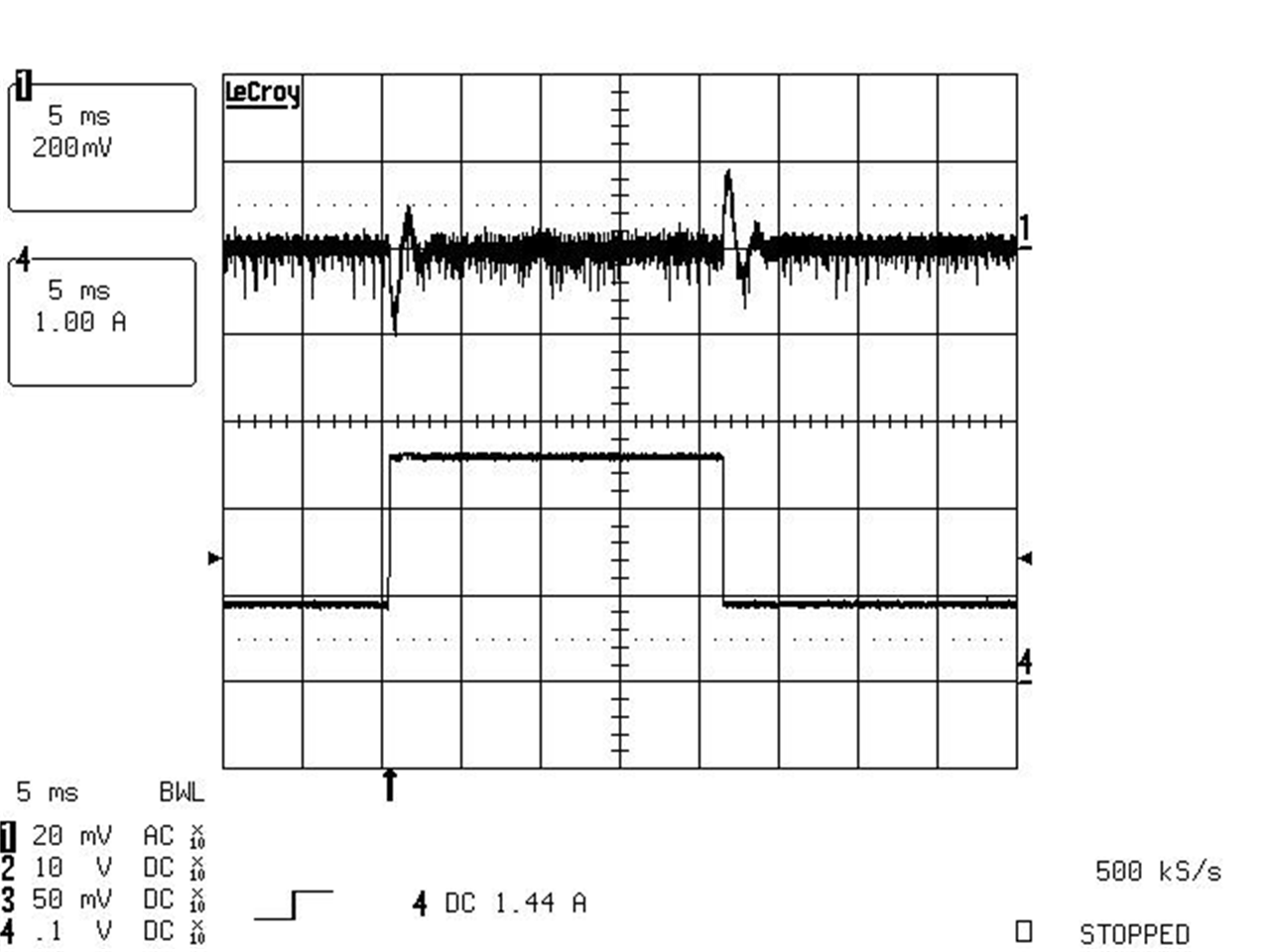 Figure 40. Output Voltage During 0.9-A to 2.7-A Load Transient (CH1: Output Voltage AC Coupled, 200 mV/div; CH4: Output Current, 1 A/div)
 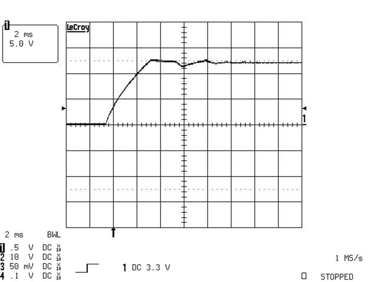 Figure 42. Output Voltage Behavior at Full Load Start-up (5 V/div)
 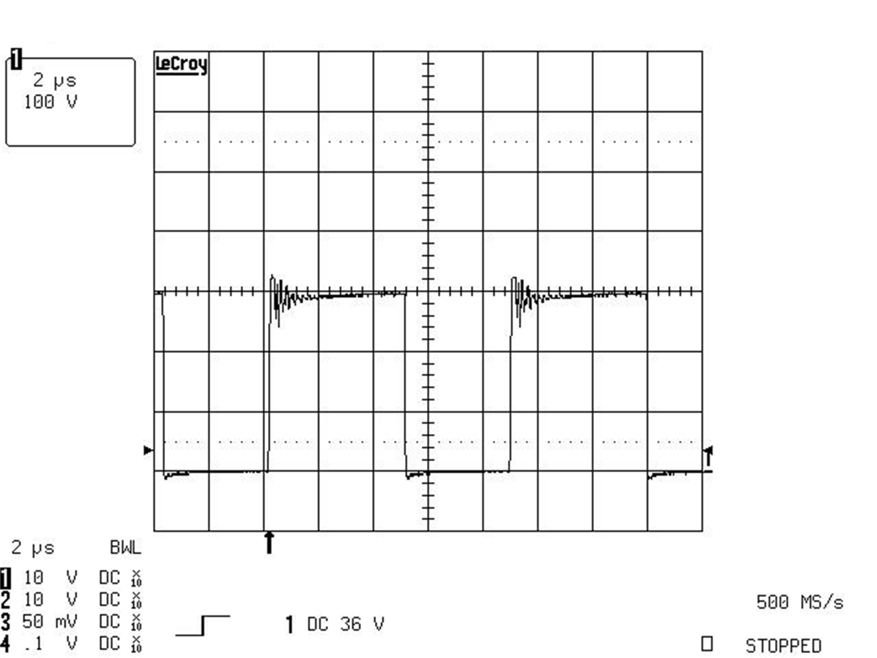 Figure 39. Primary Side MOSFET Drain to Source Voltage at 120-V AC Input (100 V/div)
 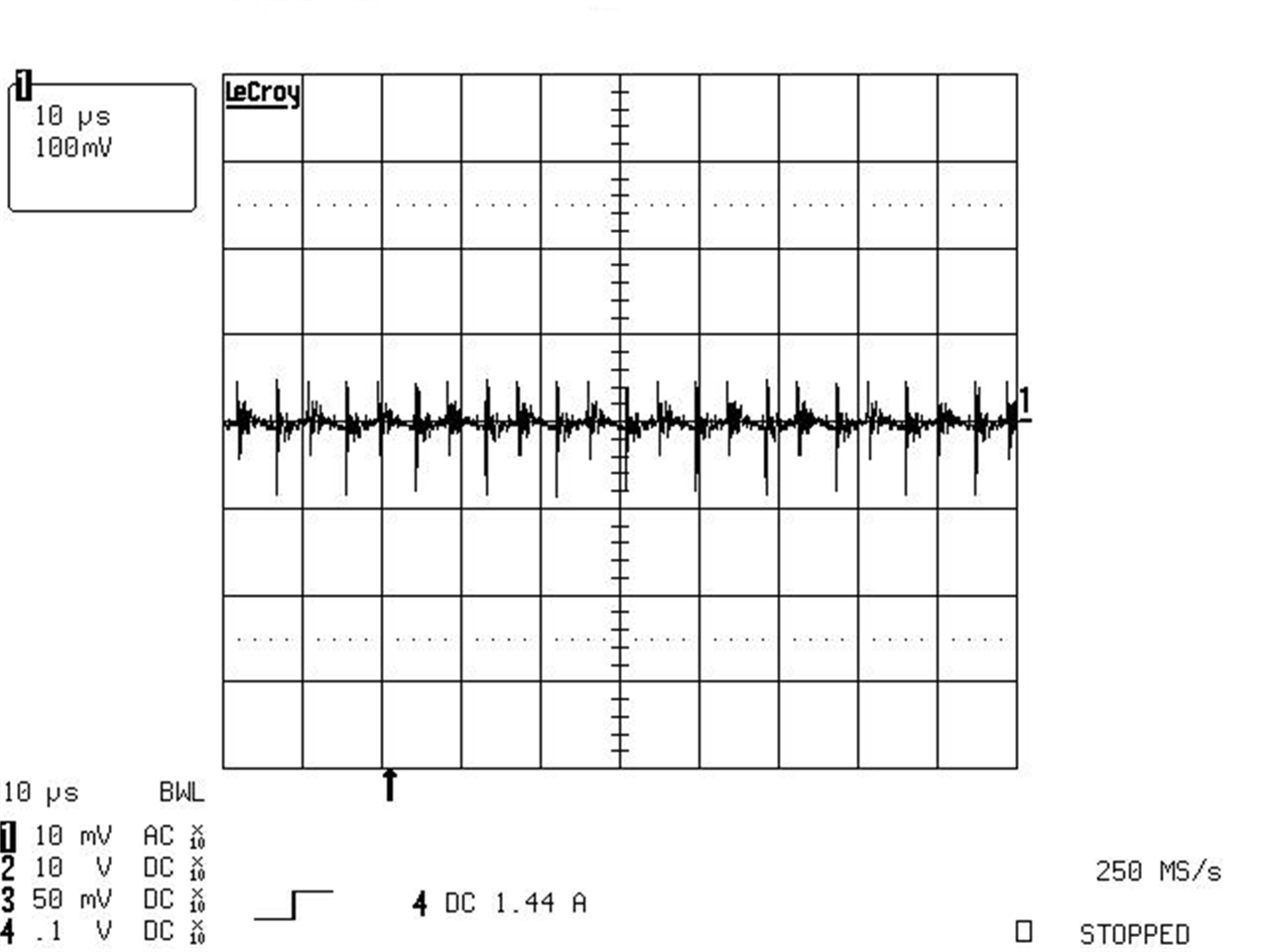 Figure 41. Output Voltage Ripple at Full Load (100 mV/div)