SLUSA29D April 2010 – August 2015 UCC28250
PRODUCTION DATA.
- 1 Features
- 2 Applications
- 3 Description
- 4 Revision History
- 5 Pin Configuration and Functions
- 6 Specifications
-
7 Detailed Description
- 7.1 Overview
- 7.2 Functional Block Diagram
- 7.3
Feature Description
- 7.3.1 VDD (5/12)
- 7.3.2 VREF (Reference Generator) (20/7)
- 7.3.3 EN (Enable Pin) (18/5)
- 7.3.4 RT (Oscillator Frequency Set and Synchronization) (15/2)
- 7.3.5 SP (Synchronous Rectifier Turnoff to Primary Output Turnon Dead Time Programming) (13/19)
- 7.3.6 PS (Primary Output Turnoff to Synchronous Rectifier Turnon Dead Time Programming) (11/18)
- 7.3.7 RAMP/CS (PWM Ramp Input or Current Sense Input) (16/3)
- 7.3.8 REF/EA+ (1/8)
- 7.3.9 FB/EA- (2/9)
- 7.3.10 COMP (3/10)
- 7.3.11 VSENSE (14/1)
- 7.3.12 SS (Soft Start Programming Pin) (13/20)
- 7.3.13 ILIM (Current Limit for Cycle-By-Cycle Overcurrent Protection) (17/4)
- 7.3.14 HICC (10/17)
- 7.3.15 OVP/OTP (19/6)
- 7.3.16 OUTA (9/16) and OUTB (8/15)
- 7.3.17 SRA (7/14) and SRB (6/13)
- 7.3.18 GND (4/11)
- 7.4 Device Functional Modes
-
8 Applications and Implementation
- 8.1 Application Information
- 8.2
Typical Applications
- 8.2.1
Design Example
- 8.2.1.1 Design Requirements
- 8.2.1.2
Detailed Design Procedure
- 8.2.1.2.1 Step 1, Power Stage Design
- 8.2.1.2.2 Step 2, Feedback Loop Design
- 8.2.1.2.3 Step 3, Programming the Device
- 8.2.1.2.4 Step 3-3, Determine Soft-Start Capacitance
- 8.2.1.2.5 Step 3-4, Determine Dead-Time Resistance
- 8.2.1.2.6 Step 3-5, Determine OCP Hiccup Off-Time Capacitance
- 8.2.1.2.7 Step 3-6, Determine Primary-Side OVP Resistance
- 8.2.1.2.8 Step 3-7, Select Capacitance for VDD and VREF
- 8.2.1.3 Application Curves
- 8.2.2 Secondary-Side Half-Bridge Controller with Synchronous Rectification
- 8.2.1
Design Example
- 9 Power Supply Recommendations
- 10Layout
- 11Device and Documentation Support
- 12Mechanical, Packaging, and Orderable Information
Package Options
Mechanical Data (Package|Pins)
Thermal pad, mechanical data (Package|Pins)
- RGP|20
Orderable Information
10 Layout
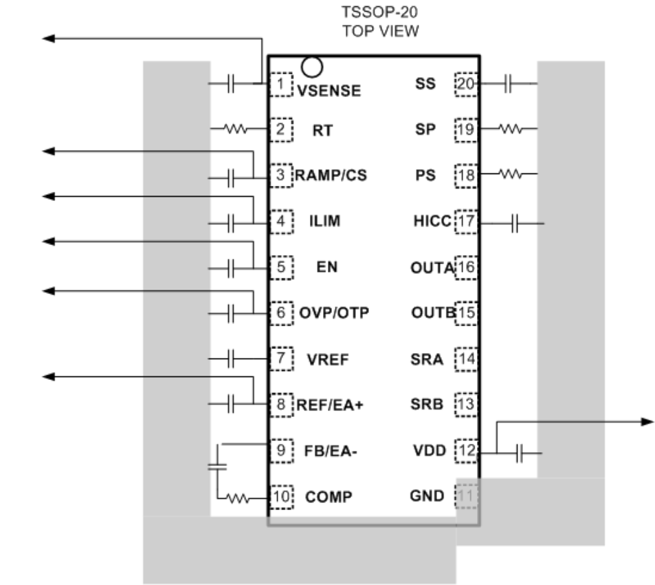
10.1 Layout Guidelines
To increase the reliability and robustness of the design, the following layout guidelines must be met.
- REF/EA+ The REF/EA+ pin is the noninverting input of the error amplifier. For secondary side control, this pin is used to set the reference of voltage loop which decides the output voltage. So it is important to keep it clear from any of high voltage switching nodes. In addition, a decoupling capacitor located closely is recommended. For primary side control, this pin must be connected to opto-coupler. it is important minimize the loop area by running the EA+ signal and GND trace in parallel.
- FB/EA- Minimize the loop between FB/EA- and COMP and keep it clear from any of high voltage switch nodes to avoid the noise injection into to the compensation loop.
- COMP Minimize the loop between FB/EA- and COMP and keep it clear from any of high voltage switch nodes to avoid the noise injection into to the compensation loop.
- GND As with all PWM controllers, the effectiveness of the filter capacitors on the signal pins depends upon the integrity of the ground return. Place all decoupling and filter capacitors as close as possible to the device pins with short traces. The AGND pin is used as the return connection for the low-power signaling and sensitive signal so it should be separated from the power stage ground to avoid ground bouncing.
- VDD, VREF The VCC pin must be decoupled to GND by minimum 1-μF ceramic capacitors placed close to the pins.
- SRA, SRB, OUTA, OUTB The SRA and SRB gate drive pins can be used to drive the inputs of gate driver or to directly drive the primary winding of a gate-drive transformer or the to directly drive the input of isolator. The tracks connected to these pins carry high dv/dt signals. Minimize noise pickup by routing them as far away as possible from tracks connected to sensitive signal including EA+, EA-, COMP, VSENSE, RT, RAMP/CS, ILIM, PS, SP.
- HICC, SS, EN, OVP/OTP The connection track between the pin and external corresponding capacitor should be short.
- PS, SP, RT, VSENSE, RAMP/CS, ILIM These pins are noise sensitive so allocate the related resistor as close as possible with the good ground connection.
10.2 Layout Example
 Figure 54. Layout Example
10.3 Thermal Protection
Internal thermal shutdown circuitry protects the UCC28250 in the event the maximum rated junction temperature is exceeded. When activated, typically at 160°C, with the maximum threshold at 170°C and minimum threshold at 150°C the controller is forced into a low power standby mode. The outputs (OUTA, OUTB, SRA, SRB) are disabled. This helps to prevent accidental device overheating. A 20°C hysteresis is added to prevent comparator oscillation. During thermal shutdown, the UCC28250 follows a normal start-up sequence after the junction temperature falls below 140°C (typical value, with 130°C minimum threshold and 150°C maximum threshold).