SLUS646K November 2005 – August 2015 UCC28600
PRODUCTION DATA.
- 1 Features
- 2 Applications
- 3 Description
- 4 Revision History
- 5 Pin Configuration and Functions
- 6 Specifications
- 7 Detailed Description
- 8 Application and Implementation
- 9 Power Supply Recommendations
- 10Layout
- 11Device and Documentation Support
- 12Mechanical, Packaging, and Orderable Information
Package Options
Refer to the PDF data sheet for device specific package drawings
Mechanical Data (Package|Pins)
- D|8
Thermal pad, mechanical data (Package|Pins)
Orderable Information
7 Detailed Description
7.1 Overview
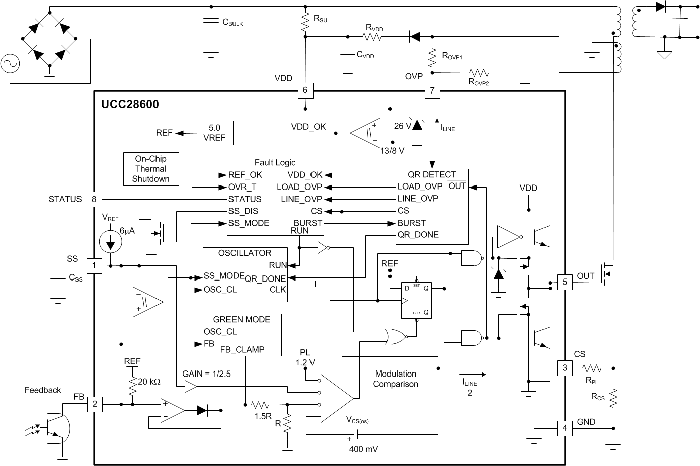
The UCC28600 is a flyback power supply controller that operates in different operating modes, modulating the peak primary current and/or the switching frequency, depending upon the line and load conditions. The controller will operate in burst mode operation, or green mode (GM) driving the primary side MOSFET with packets of
40-kHz pulses, at fixed peak primary current for light-load conditions. As the load increases, the 40-kHz switching will become consistent and the controller will transition to frequency fold-back mode (FFM), where the peak primary current is held constant and the switching frequency is modulated from 40 kHz up to 130 kHz, in order to maintain regulation. At higher loads, the UCC28600 will operate in either DCM, where the peak primary current is modulated but the switching frequency is maintained at its maximum value, or quasi-resonant mode (QRM), where the switching frequency and the peak primary current are both modulated in order to maintain regulation.
7.2 Functional Block Diagram
7.2.1 Terminal Components
Table 1. Terminal Components
| PIN | I/O | DESCRIPTION (1)(2) | |
|---|---|---|---|
| NAME | NO. | ||
| CS | 3 | I |
Equation 1.
 Equation 2. where: 
|
| FB | 2 | I | Opto-isolator collector |
| GND | 4 | – | Bypass capacitor to VDD, CBP = 0.1 μF |
| OUT | 5 | O | Power MOSFET gate |
| OVP | 7 | I |
Equation 3.
 Equation 4. where: 
|
| SS | 1 | I |
Equation 5. where tSS(min) is the greater of:  Equation 6.
 or Equation 7.

|
| STATUS | 8 | O |
Equation 8.
 Equation 9. where: 
|
| VDD | 6 | I |
CVDD is the greater of: Equation 10.
 or Equation 11.
 Equation 12.
 Equation 13. where:
|
7.3 Feature Description
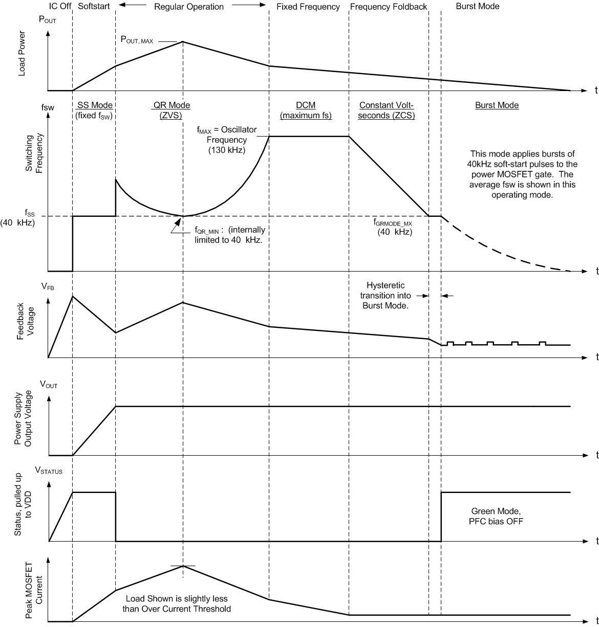
The UCC28600 is a multi-mode controller, as illustrated in Figure 5 and Figure 12. The mode of operation depends upon line and load conditions. Under all modes of operation, the UCC28600 terminates the OUT = HI signal based on the switch current. Thus, the UCC28600 always operates in current mode control so that the power MOSFET current is always limited.
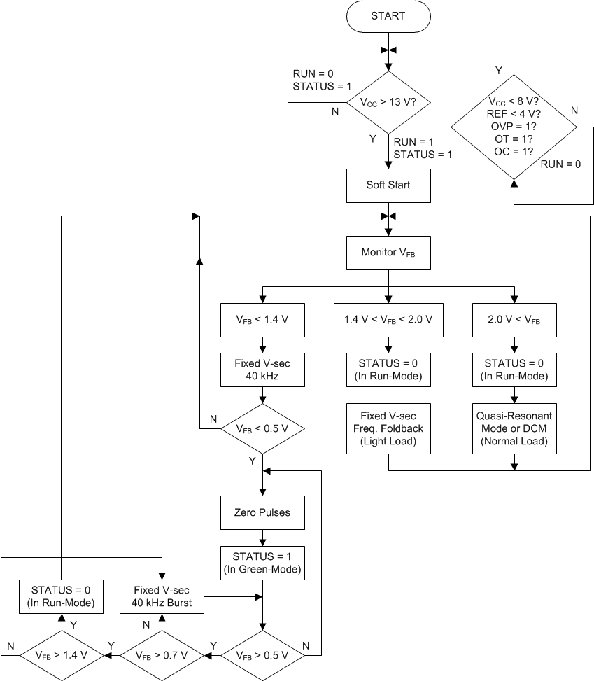
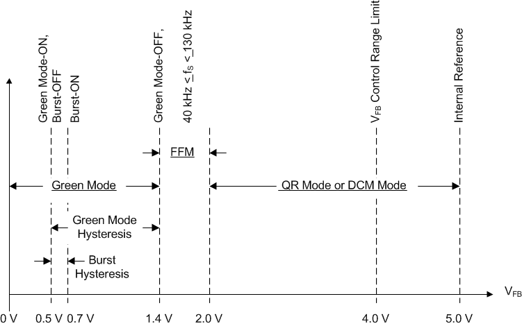
Under normal operating conditions, the FB pin commands the operating mode of the UCC28600 at the voltage thresholds shown in the control flow chart, Figure 11. Soft-start and fault responses are the exception. During soft start, the converter switching frequency is fixed at 40 kHz and FB is set to 5V. The soft-start mode is latched-OFF when VSS becomes greater than VFB for the first time after UVLOON. The soft-start state cannot be recovered until after passing UVLOOFF, and then, UVLOON.
From 100% to approximately 30% full rated power the UCC28600 controls the converter in quasi-resonant mode (QRM) or discontinuous conduction mode (DCM), where DCM operation is at the clamped maximum switching frequency (130 kHz). For loads that are between approximately 30% and 10% full rated power, the converter operates in frequency foldback mode (FFM), where the peak switch current is constant and the output voltage is regulated by modulating the switching frequency for a given and fixed VIN. Effectively, operation in FFM results in the application of constant volt-seconds to the flyback transformer each switching cycle. Voltage regulation in FFM is achieved by varying the switching frequency in the range from 130 kHz to 40 kHz. For extremely light loads (below approximately 10% full rated power), the converter is controlled using bursts of 40-kHz pulses.
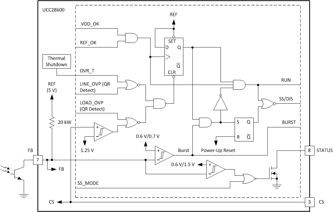
Details of the functional boxes in the Block Diagram/Typical Application drawing are shown in Figure 8, Figure 6, Figure 7 and Figure 10. These figures conceptualize how the UCC28600 executes the command of the FB voltage to have the responses that are shown in Figure 11, Figure 5 and Figure 12. The details of the functional boxes also conceptualize the various fault detections and responses that are included in the UCC28600. During all modes of operation, this controller operates in current mode control. This allows the UCC28600 to monitor the FB voltage to determine and respond to the varying load levels such as heavy, light or ultra-light.
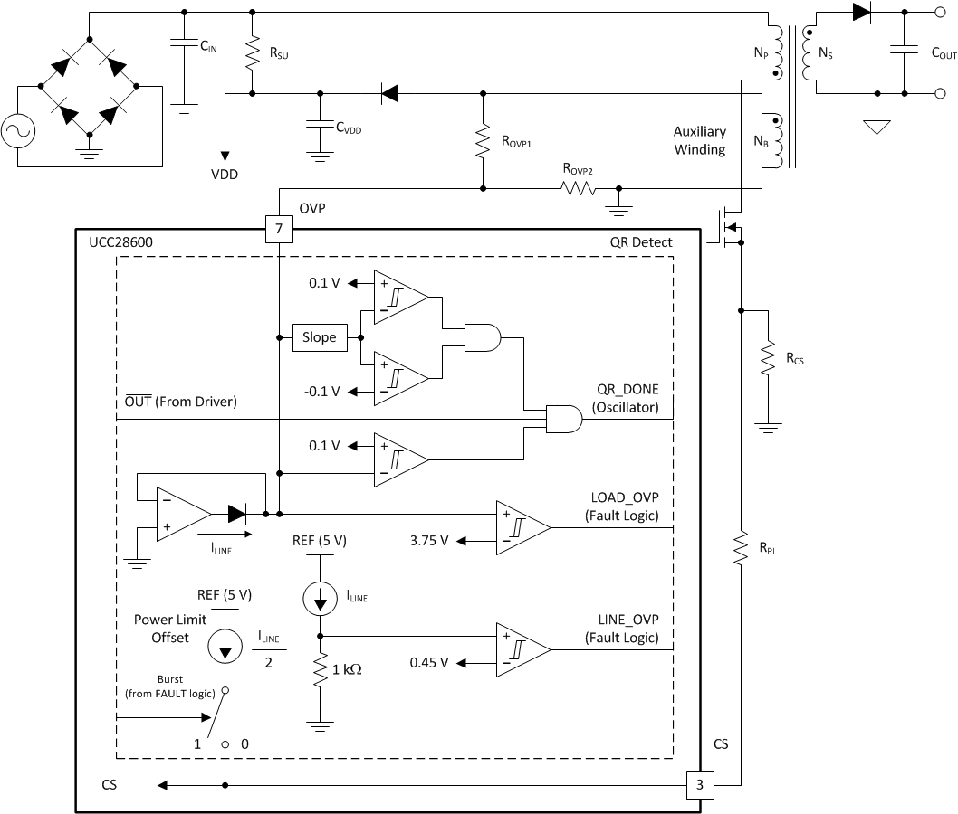
Quasi-resonant mode and DCM occurs for feedback voltages VFB between 2.0 V and 4.0 V, respectively. In turn, the CS voltage is commanded to be between 0.4 V and 0.8 V. A cycle-by-cycle power limit imposes a fixed 0.8-V limit on the CS voltage. An overcurrent shutdown threshold in the fault logic gives added protection against high-current, slew-rate shorted winding faults, shown in Figure 10. The power limit feature in the QR DETECT circuit of Figure 7 adds an offset to the CS signal that is proportional to the line voltage. The power limit feature is programmed with RPL, as shown in the Typical Application Diagram.
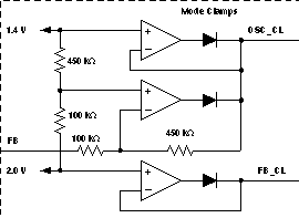 Figure 6. Mode Clamp Details
7.3.1 Oscillator
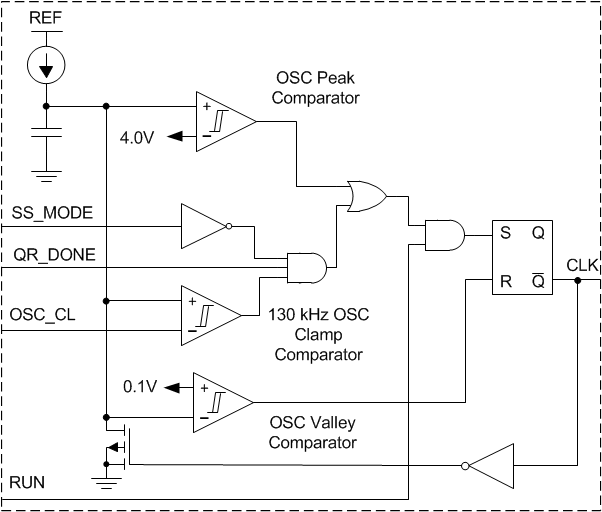
The oscillator, shown in Figure 8, is internally set and trimmed so it is clamped by the circuit in Figure 8 to a nominal 130-kHz maximum operating frequency. It also has a minimum frequency clamp of 40 kHz. If the FB voltage tries to drive operation to less than 40 kHz, the converter operates in green mode.
7.3.2 Status
The STATUS pin is an open drain output, as shown in Figure 10. The status output goes into the OFF-state when FB falls below 0.5 V and it returns to the ON-state (low impedance to GND) when FB rises above 1.4 V. This pin is used to control bias power for a PFC stage, as shown in Figure 9. Key elements for implementing this function include Q1, RST1 and RST2, as shown in Figure 9. Resistors RST1 and RST2 are selected to saturate Q1 when it is desirable for the PFC to be operational. During green mode, the STATUS pin becomes a high impedance and RST2 causes Q1 to turn-OFF, thus saving bias power. If necessary, use a Zener diode and a resistor (DZ1 and RVCC) to maintain VCC in the safe operating range of the PFC controller.
NOTE
The DVDD – CVDD combination is in addition to the standard DBIAS – CBIAS components.
This added stage is required to isolate the STATUS circuitry from the start-up resistor, RSU, to ensure there is no conduction through STATUS when VDD is below the UVLO turn-on threshold.
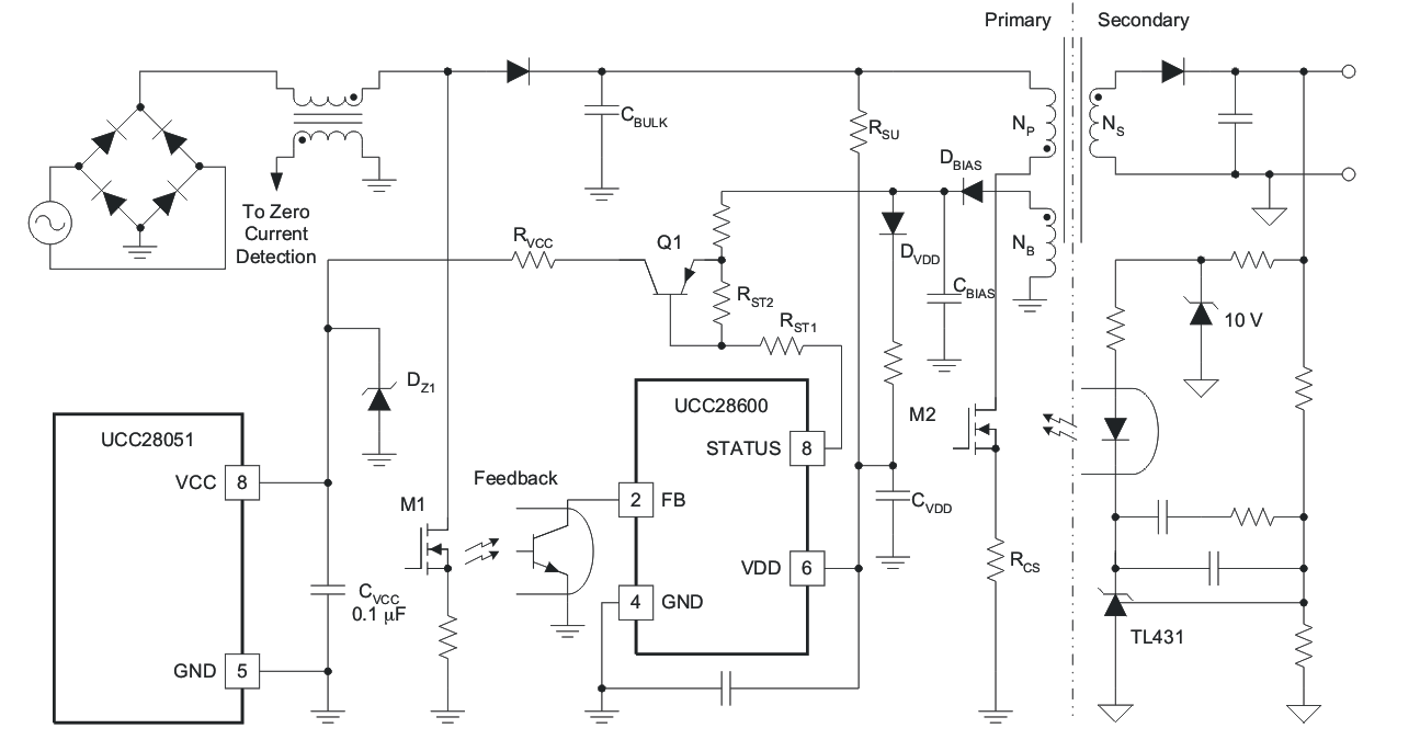 Figure 9. Using STATUS for PFC Shut-Down During Green Mode
7.3.3 Fault Logic
Advanced logic control coordinates the fault detections to provide proper power supply recovery. This provides the conditioning for the thermal protection. Line overvoltage protection (line OVP) and load OVP are implemented in this block. It prevents operation when the internal reference is below 4.5 V. If a fault is detected in the thermal shutdown, line OVP, load OVP, or REF, the UCC28600 undergoes a shutdown/retry cycle.
Refer to the fault logic diagram in Figure 10 and the QR detect diagram in Figure 7 to program line OVP and load OVP. To program the load OVP, select the ROVP1 – ROVP2 divider ratio to be 3.75 V at the desired output shut-down voltage. To program line OVP, select the impedance of the ROVP1 – ROVP2 combination to draw 450 μA when the VOVP is 0.45 V during the ON-time of the power MOSFET at the highest allowable input voltage.
7.3.4 Protection Features
The UCC28600 has many protection features that are found only on larger, full featured controllers. Refer to the Functional Block Diagram, Typical Application Diagram, Figure 6, Figure 7, Figure 8, Figure 10, Figure 11, and Figure 12 for detailed block descriptions that show how the features are integrated into the normal control functions.
7.3.5 Overtemperature
Overtemperature lockout typically occurs when the substrate temperature reaches 140°C. Retry is allowed if the substrate temperature reduces by the hysteresis value. Upon an overtemperature fault, CSS on softstart is discharged and STATUS is forced to a high impedance.
7.3.6 Cycle-by-Cycle Power Limit
The cycle terminates when the CS voltage plus the power limit offset exceeds 1.2 V.
In order to have power limited over the full line voltage range of the QR Flyback converter, the CS pin voltage must have a component that is proportional to the primary current plus a component that is proportional to the line voltage due to predictable switching frequency variations due to line voltage. At power limit, the CS pin voltage plus the internal CS offset is compared against a constant 1.2-V reference in the PWM comparator. Thus during cycle-by-cycle power limit, the peak CS voltage is typically 0.8 V.
The current that is sourced from the OVP pin (ILINE) is reflected to a dependent current source of ½ ILINE, that is connected to the CS pin. The power limit function can be programmed by a resistor, RPL, that is between the CS pin and the current sense resistor. The current, ILINE, is proportional to line voltage by the transformer turns ratio NB/NP and resistor ROVP1. Current ILINE is programmed to set the line over voltage protection. Resistor RPL results in the addition of a voltage to the current sense signal that is proportional to the line voltage. The proper amount of additional voltage has the effect of limiting the power on a cycle-by-cycle basis. Note that RCS, RPL, ROVP1 and ROVP2 must be adjusted as a set due to the functional interactions.
7.3.7 Primary Current Protection
When the primary current exceeds maximum current level which is indicated by a voltage of 1.25 V at the CS pin, the device initiates a shutdown. Retry occurs after a UVLOOFF or UVLOON cycle. Because the device will initiate cycle-by-cycle power limit first, primary side current protection is not intended to protect against output short circuit conditions. However, this feature does protect the MOSFET against extreme conditions such as transformer saturation.
7.3.8 Over-Voltage Protection
Line and load over voltage protection is programmed with the transformer turn ratios, ROVP1 and ROVP2. The OVP pin has a 0-V voltage source that can only source current; OVP cannot sink current.
Line over voltage protection occurs when the OVP pin is clamped at 0 V. When the bias winding is negative, during OUT = HI or portions of the resonant ring, the 0-V voltage source clamps OVP to 0 V and the current that is sourced from the OVP pin is mirrored to the Line_OVP comparator and the QR detection circuit. The Line_OVP comparator initiates a shutdown-retry sequence if OVP sources any more than 450 μA.
Load-over voltage protection occurs when the OVP pin voltage is positive. When the bias winding is positive, during demagnetization or portions of the resonant ring, the OVP pin voltage is positive. If the OVP voltage is greater than 3.75 V, the device initiates a shutdown. Retry occurs after a UVLOOFF or UVLOON cycle.
7.3.9 Undervoltage Lockout
Protection is provided to guard against operation during unfavorable bias conditions. Undervoltage lockout (UVLO) always monitors VDD to prevent operation below the UVLO threshold.
7.4 Device Functional Modes
Depending upon the line and load conditions, the UCC28600 controls the converter using different modes of operation, which are defined as quasi-resonant (QR mode), discontinuous conduction mode (DCM), frequency foldback mode (FFM) and green mode (GM), determined by the voltage on the FB pin, as shown in Figure 11.
For extremely light loads (below approximately 10% full rated power), the converter is controlled using bursts of 40-kHz pulses. As the load increases, the number of pulses in these burst packets increases until the converter is switching consistently at 40 kHz, at which point it transitions into the next operating mode, called frequency foldback. Frequency foldback mode (FFM) typically begins at loads that are between approximately 10% and up to 30% full rated power, the peak primary side switch current is constant and the output voltage is regulated by modulating the switching frequency from 40 kHz up to 130 kHz. From approximately 30% to 100% full rated power, the UCC28600 controls the converter in either quasi-resonant mode (QRM) or discontinuous conduction mode (DCM). In QRM, the switching frequency will decrease as the load increases; DCM operation is at the clamped maximum switching frequency (130 kHz). The valley detection circuitry is active during FFM, DCM, and QRM operation.
Keep in mind that the aforementioned boundaries of steady-state operation are approximate because they are subject to converter design parameters.
7.4.1 Quasi-Resonant and DCM Control
During this control mode, the rising edge of OUT will occur just after the valley of the resonant ring when the transformer is fully demagnetized. Resonant valley switching is an integral part of QR operation. In this mode, the flyback converter operates at the boundary of discontinuous conduction mode and continuous conduction mode. By adjusting both the peak current and the switching frequency, the output power is adjusted to match the load requirement. When the load increases, the peak current increases and the switching frequency decreases. The minimum switching frequency of the converter is limited to 40 kHz. The transformer magnetizing inductor value has to be designed accordingly so that the converter can deliver the maximum required power while maintaining a switching frequency that is greater than the fQR(min) over the entire input operating range.
As the load decreases from its designed maximum output power, the UCC28600 will demand a higher switching frequency and decreased peak current. The converter’s maximum switching frequency will be limited to 130 kHz. At this maximum switching frequency, the converter enters DCM control. At DCM control, the peak current is adjusted to control the output power. Slight frequency dithering between resonant valleys will occur as the valley detection is active in DCM control.
Quasi-resonant (QR) and DCM operation occur for feedback voltages, VFB, between 2.0 V and 3.0 V. In turn, the peak CS voltage is commanded to be between 0.4 V and 0.8 V. The CS pin has an internal dependent current source, 1/2 ILINE. This current source adds a proportional step offset (power limit offset) to the CS signal and is part of the cycle-by-cycle power limit function that is discussed in the Protection Features section.
7.4.2 Frequency Foldback Mode Control
Operation in FFM results in the application of constant volt-seconds to the flyback transformer during each switching cycle. During frequency foldback mode, as the load decreases, the MOSFET peak current is kept constant and the switching frequency is reduced (foldback) to reduce the output power. In this mode, the flyback converter will always operate in discontinuous conduction mode. When the FB voltage is between 1.4 V and
2.0 V, the voltage controlled oscillator restricts the operating frequency between 40 kHz and 130 kHz and the CS is clamped to 0.4 V, including the power limit offset. Valley detection is active during FFM.
7.4.3 Green-Mode Control
During green mode, the converter operates at a fixed switching frequency of 40 kHz and fixed peak current. The output power is adjusted by the converter ON/OFF durations, which is also known as burst mode. When the FB voltage is between 1.4 V and 0.5 V, the controller is commanding an excess of energy to be transferred to the load which in turn, drives the error higher and FB lower. When FB reaches 0.5 V, the OUT pulses are terminated and do not resume until FB reaches 0.7 V. In this mode, the converter operates in hysteretic control with the OUT pulse terminated at a fixed CS voltage level of 0.4 V. The power limit offset is turned OFF during Green mode and it returns to ON when FB is above 1.4 V. Green mode reduces the average switching frequency in order to minimize switching losses and increase the efficiency at light-load conditions.
7.4.4 Operating Mode Programming
Boundaries of the operating modes are programmed by the flyback transformer and the four components RPL, RCS, ROVP1 and ROVP2; shown in the Functional Block Diagram and Typical Application Diagram drawing.
The transformer characteristics that predominantly affect the modes are the magnetizing inductance of the primary and the magnitude of the output voltage, reflected to the primary. To a lesser degree (yet significant), the boundaries are affected by the MOSFET output capacitance and transformer leakage inductance. The design procedure here is to select a magnetizing inductance and a reflected output voltage that operates at the DCM/CCM boundary at maximum load and maximum line. The actual inductance should be noticeably smaller to account for the ring between the magnetizing inductance and the total stray capacitance measured at the drain of the power MOSFET. This programs the QR/DCM boundary of operation. All other mode boundaries are preset with the thresholds in the oscillator and green-mode blocks.
The four components RPL, RCS, ROVP1 and ROVP2 must be programmed as a set due to the interactions of the functions. The use of the UCC28600 design calculator, SLVC104, is highly recommended in order to achieve the desired results with a careful balance between the transformer parameters and the programming resistors.
