SLUSBW3D March 2014 – December 2017 UCC28630 , UCC28631 , UCC28632 , UCC28633 , UCC28634
PRODUCTION DATA.
- 1 Features
- 2 Applications
- 3 Description
- 4 Revision History
- 5 Device Comparison Table
- 6 Pin Configuration and Functions
- 7 Specifications
-
8 Detailed Description
- 8.1 Overview
- 8.2 Functional Block Diagram
- 8.3
Feature Description
- 8.3.1 High-Voltage Current Source Start-Up Operation
- 8.3.2 AC Input UVLO / Brownout Protection
- 8.3.3 Active X-Capacitor Discharge (UCC28630 and UCC28633 only)
- 8.3.4 Magnetic Input and Output Voltage Sensing
- 8.3.5 Fixed-Point Magnetic Sense Sampling Error Sources
- 8.3.6 Magnetic Sense Resistor Network Calculations
- 8.3.7 Magnetic Sensing: Power Stage Design Constraints
- 8.3.8 Magnetic Sense Voltage Control Loop
- 8.3.9 Peak Current Mode Control
- 8.3.10 IPEAK Adjust vs. Line
- 8.3.11 Primary-Side Constant-Current Limit (CC Mode)
- 8.3.12 Primary-Side Overload Timer (UCC28630 only)
- 8.3.13 Overload Timer Adjustment (UCC28630 only)
- 8.3.14 CC-Mode IOUT(lim) Adjustment
- 8.3.15 Fault Protections
- 8.3.16 Pin-Fault Detection and Protection
- 8.3.17 Over-Temperature Protection
- 8.3.18 External Fault Input
- 8.3.19 External SD Pin Wake Input (except UCC28633)
- 8.3.20 External Wake Input at VSENSE Pin (UCC28633 Only)
- 8.3.21 Mode Control and Switching Frequency Modulation
- 8.3.22 Frequency Dither For EMI (except UCC28632)
- 8.4 Device Functional Modes
-
9 Applications and Implementation
- 9.1 Application Information
- 9.2
Typical Application
- 9.2.1 Notebook Adapter, 19.5 V, 65 W
- 9.2.2 UCC28630 Application Schematic
- 9.2.3 Design Requirements
- 9.2.4
Detailed Design Procedure
- 9.2.4.1 Custom Design With WEBENCH® Tools
- 9.2.4.2 Input Bulk Capacitance and Minimum Bulk Voltage
- 9.2.4.3 Transformer Turn Ratio
- 9.2.4.4 Transformer Magnetizing Inductance
- 9.2.4.5 Current Sense Resistor RCS
- 9.2.4.6 Transformer Constraint Verification
- 9.2.4.7 Transformer Selection and Design
- 9.2.4.8 Slope Compensation Verification
- 9.2.4.9 Power MOSFET and Output Rectifier Selection
- 9.2.4.10 Output Capacitor Selection
- 9.2.4.11 Calculation of CC Mode Limit Point
- 9.2.4.12 VDD Capacitor Selection
- 9.2.4.13 Magnetic Sense Resistor Network Selection
- 9.2.4.14 Output LED Pre-Load Resistor Calculation
- 9.2.5 External Wake Pulse Calculation at VSENSE Pin (UCC28633 Only)
- 9.2.6 Energy Star Average Efficiency and Standby Power
- 9.2.7 Application Performance Plots
- 9.3 Dos and Don'ts
- 10Power Supply Recommendations
- 11Layout
- 12Device and Documentation Support
- 13Mechanical, Packaging, and Orderable Information
Package Options
Mechanical Data (Package|Pins)
- D|7
Thermal pad, mechanical data (Package|Pins)
Orderable Information
8.3.9 Peak Current Mode Control
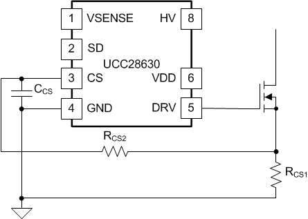
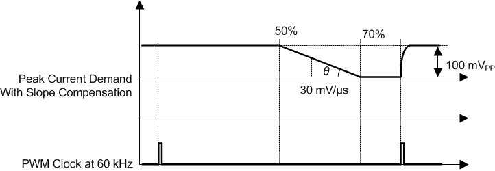
The controller operates in peak current mode. The primary-side switch (MOSFET) current is sensed by a shunt resistor (RCS1) connected in series with the source of the FET as shown in Figure 30. The voltage that is developed across the sense resistor is connected to the CS pin of the controller. The device uses the current sense signal at the CS pin to terminate the PWM pulse according to the peak current demand of the modulator. The device automatically applies slope compensation as soon as the duty cycle of the DRV pin pulse exceeds 50%. This compensation provides stable operation up to maximum DRV duty cycle. The device applies this slope compensation as a downslope on the demand signal at the PWM comparator, so is not measureable at the CS pin. The device synchronizes the slope compensation signal to the PWM and is active only between 50% and 70% duty cycle, as shown in Figure 31.
Normal operating range for the CS pin is between 0 mV and 800 mV. The RCS1 resistor should be scaled such that the peak current at maximum peak load and minimum bulk capacitor voltage produces a signal of approximately 800 mV peak at the CS pin. This resistor value is calculated in conjunction with the calculation of the required primary magnetizing inductance, as outlined in Notebook Adapter, 19.5 V, 65 W, section.
 Figure 30. Primary-Side Current Sensing
 A nominal 100 ns of filtering that is internal to the CS pin helps filter the leading turn-on spike of current. Depending on PCB layout, an RC filter (RCS2 and CCS) may be required on the CS pin as shown in Figure 30 to filter noise and spikes. The capacitor CCS should be positioned as close as possible to pins 3 and 4 and tracked directly to the pins. Series resistor RCS2 should also be located close to pin 3 to minimize noise pick-up. RCS2 value should not exceed 20 kΩ, because a larger value could be detected as a possible open circuit on the CS pin during the start-up pin-fault checks. The R-C filter time constant should not be excessive (timing between 100 ns and 200 ns is typical). Otherwise the filter reduces the measured peak current, and allows greater actual peak current to flow versus the modulator demand level. Such effects force the regulation loop to reduce the switching frequency to compensate, and at highest line, no load, this can lead to regulation difficulties if the control loop attempts to drop the frequency so far that it reaches the fMIN limit.
 Figure 31. Peak Current Demand with Slope Compensating Downslope