SLUSB41A July 2012 – December 2014 UCC28700 , UCC28701 , UCC28702 , UCC28703
PRODUCTION DATA.
- 1 Features
- 2 Applications
- 3 Description
- 4 Revision History
- 5 Device Comparison Table
- 6 Pin Configuration and Functions
- 7 Specifications
- 8 Detailed Description
-
9 Applications and Implementation
- 9.1 Application Information
- 9.2
Typical Application
- 9.2.1 Design Requirements
- 9.2.2
Detailed Design Procedure
- 9.2.2.1 Transformer Parameter Verification
- 9.2.2.2 Output Capacitance
- 9.2.2.3 VDD Capacitance, CDD
- 9.2.2.4 VDD Start-Up Resistance, RSTR
- 9.2.2.5 VS Resistor Divider, Line Compensation, and Cable Compensation
- 9.2.2.6 Input Bulk Capacitance and Minimum Bulk Voltage
- 9.2.2.7 Transformer Turns Ratio, Inductance, Primary-Peak Current
- 9.2.2.8 Standby Power Estimate
- 9.2.3 Application Curves
- 10Power Supply Recommendations
- 11Layout
-
12Device and Documentation Support
- 12.1
Device Support
- 12.1.1
Device Nomenclature
- 12.1.1.1 Capacitance Terms in Farads
- 12.1.1.2 Duty Cycle Terms
- 12.1.1.3 Frequency Terms in Hertz
- 12.1.1.4 Current Terms in Amperes
- 12.1.1.5 Current and Voltage Scaling Terms
- 12.1.1.6 Transformer Terms
- 12.1.1.7 Power Terms in Watts
- 12.1.1.8 Resistance Terms in Ω
- 12.1.1.9 Timing Terms in Seconds
- 12.1.1.10 Voltage Terms in Volts
- 12.1.1.11 AC Voltage Terms in VRMS
- 12.1.1.12 Efficiency Terms
- 12.1.1
Device Nomenclature
- 12.2 Documentation Support
- 12.3 Trademarks
- 12.4 Electrostatic Discharge Caution
- 12.5 Glossary
- 12.1
Device Support
- 13Mechanical, Packaging, and Orderable Information
Package Options
Mechanical Data (Package|Pins)
- DBV|6
Thermal pad, mechanical data (Package|Pins)
Orderable Information
9 Applications and Implementation
NOTE
Information in the following applications sections is not part of the TI component specification, and TI does not warrant its accuracy or completeness. TI’s customers are responsible for determining suitability of components for their purposes. Customers should validate and test their design implementation to confirm system functionality.
9.1 Application Information
The UCC2870x family of flyback power supply controllers provides constant voltage (CV) and constant current (CC) output regulation to help meet USB-compliant adaptors and charger requirements. These devices use the information obtained from auxiliary winding sensing (VS) to control the output voltage and do not require optocoupler/TL431 feedback circuitry. Not requiring optocoupler feedback reduces the component count and makes the design more cost effective.
9.2 Typical Application
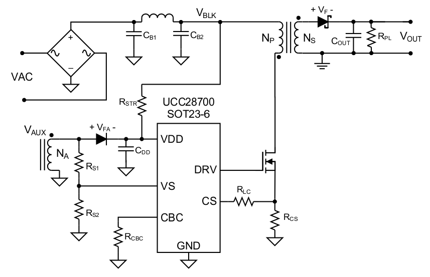 Figure 19. Typical Application Circuit
9.2.1 Design Requirements
Table 1. Design Parameters
| PARAMETER | SYMBOL | NOTES AND CONDITIONS | MIN | NOM | MAX | UNIT |
|---|---|---|---|---|---|---|
| INPUT CHARACTERISTICS | ||||||
| Input Voltage | VIN | 100 | 115/230 | 240 | V | |
| Line Frequency | fLINE | 47 | 50/60 | 64 | Hz | |
| No Load Input Power | PSB_CONV | VIN = Nom, IO = 0A | 30 | mW | ||
| Brownout Voltage | VIN(RUN) | IO = Nom | 70 | V | ||
| OUTPUT CHARACTERISTICS | ||||||
| Output Voltage | VO | VIN = Nom, IO = Nom | 4.75 | 5 | 5.25 | V |
| Output Voltage Ripple | VRIPPLE | VIN = Nom, IO = Max | 0.1 | V | ||
| Output Current | IO | VIN = Min to Max | 1 | 1.05 | A | |
| Output OVP | VOVP | IOUT = Min to Max | 5.75 | V | ||
| Transient Response | ||||||
| Load Step (VO = 4.1 V to 6 V) | VOΔ | (0.1 to 0.6 A) or (0.6 to 0.1 A) VOΔ = 0.9 V for COUT calculation in applications section |
4.1 | 5 | 6 | A |
| SYSTEMS CHARACTERISTICS | ||||||
| Switching Frequency | 105 | kHz | ||||
| Full Load Efficiency (115/230 V RMS Input) | η | IO = 1 A | 74% | 76% | ||
9.2.2 Detailed Design Procedure
This procedure outlines the steps to design a constant-voltage, constant-current flyback converter using the UCC28700 family of controllers. Please refer to the Figure 19 for circuit details and section Device Nomenclature for variable definitions used in the applications equations below.
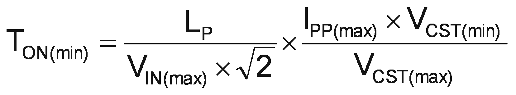
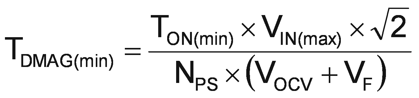
9.2.2.1 Transformer Parameter Verification
The transformer turns ratio selected affects the MOSFET VDS and secondary rectifier reverse voltage so these should be reviewed. The UCC28700 controller requires a minimum on time of the MOSFET (TON) and minimum DMAG time (TDMAG) of the secondary rectifier in the high line, minimum load condition. The selection of FMAX, LP and RCS affects the minimum TON and TDMAG.
The secondary rectifier and MOSFET voltage stress can be determined by the equations below.
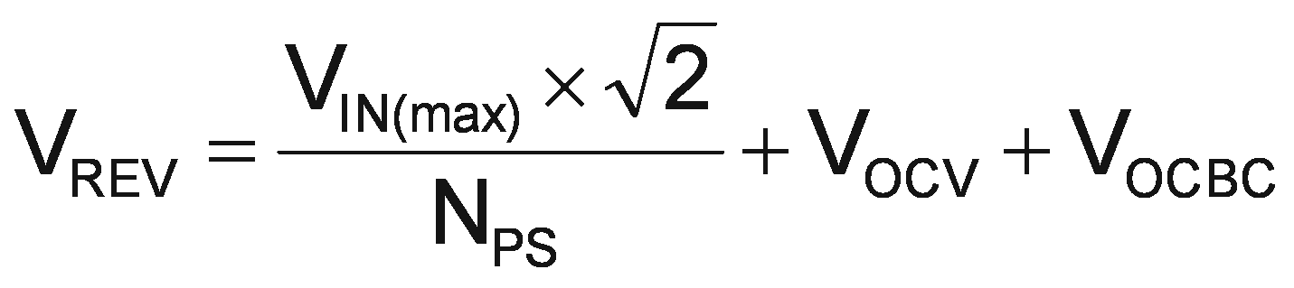
For the MOSFET VDS voltage stress, an estimated leakage inductance voltage spike (VLK) needs to be included.

The following equations are used to determine if the minimum TON target of 300 ns and minimum TDMAG target of 1.1 µs is achieved.
9.2.2.2 Output Capacitance
The output capacitance value is typically determined by the transient response requirement from no-load. For example, in some USB charger applications there is a requirement to maintain a minimum VO of 4.1 V with a load-step transient of 0 mA to 500 mA . The equation below assumes that the switching frequency can be at the UCC28700 minimum of fSW(min).
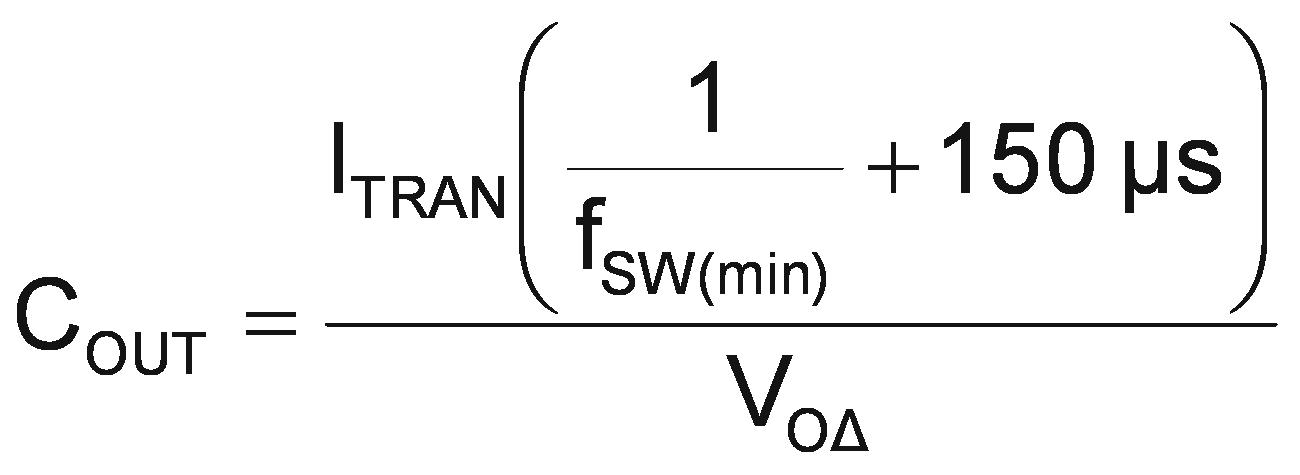
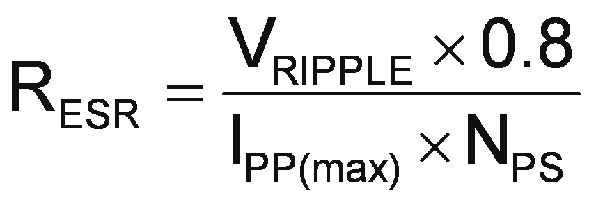
Another consideration of the output capacitor(s) is the ripple voltage requirement which is reviewed based on secondary peak current and ESR. A margin of 20% is added to the capacitor ESR requirement in the equation below.
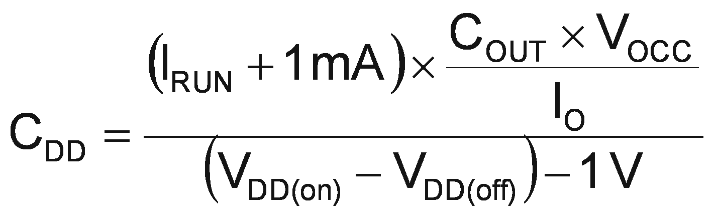
9.2.2.3 VDD Capacitance, CDD
The capacitance on VDD needs to supply the device operating current until the output of the converter reaches the target minimum operating voltage in constant-current regulation. At this time the auxiliary winding can sustain the voltage to the UCC28700. The total output current available to the load and to charge the output capacitors is the constant-current regulation target. The equation below assumes the output current of the flyback is available to charge the output capacitance until the minimum output voltage is achieved. There is an estimated 1 mA of gate-drive current in the equation and 1 V of margin added to VDD.
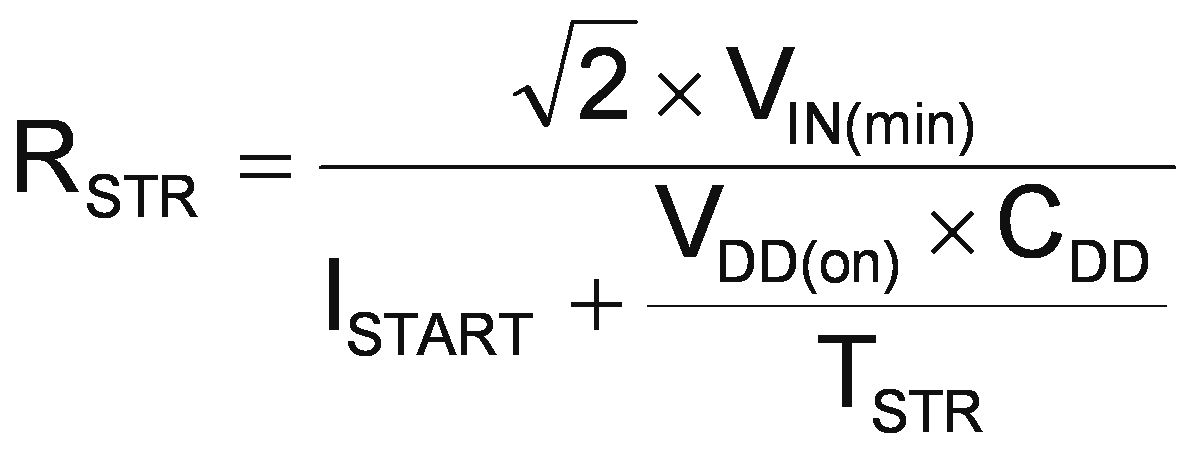
9.2.2.4 VDD Start-Up Resistance, RSTR
Once the VDD capacitance is known, the start-up resistance from VBULK to achieve the turn-on time target can be determined.
9.2.2.5 VS Resistor Divider, Line Compensation, and Cable Compensation
The VS divider resistors determine the output voltage regulation point of the flyback converter, also the high-side divider resistor (RS1) determines the line voltage at which the controller enables continuous DRV operation. RS1 is initially determined based on transformer auxiliary to primary turns ratio and desired input voltage operating threshold.
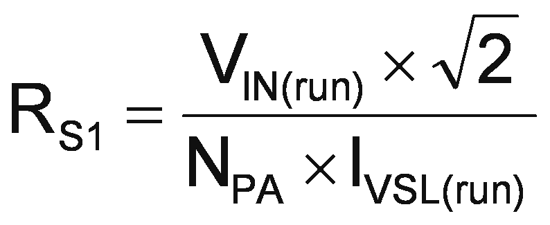
The low-side VS pin resistor is selected based on desired VO regulation voltage.
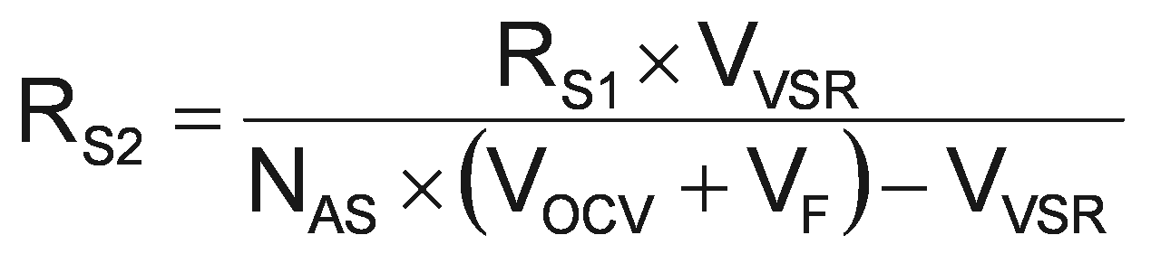
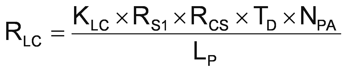
The UCC28700 can maintain tight constant-current regulation over input line by utilizing the line compensation feature. The line compensation resistor (RLC) value is determined by current flowing in RS1 and expected gate drive and MOSFET turn-off delay. Assume a 50-ns internal delay in the UCC28700.
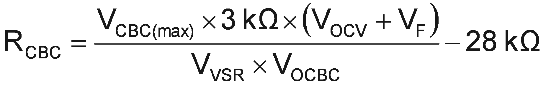
On the UCC28700 which has adjustable cable compensation, the resistance for the desired compensation level at the output terminals can be determined using the equation below.
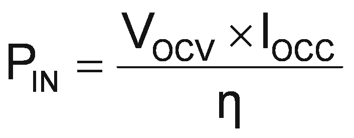
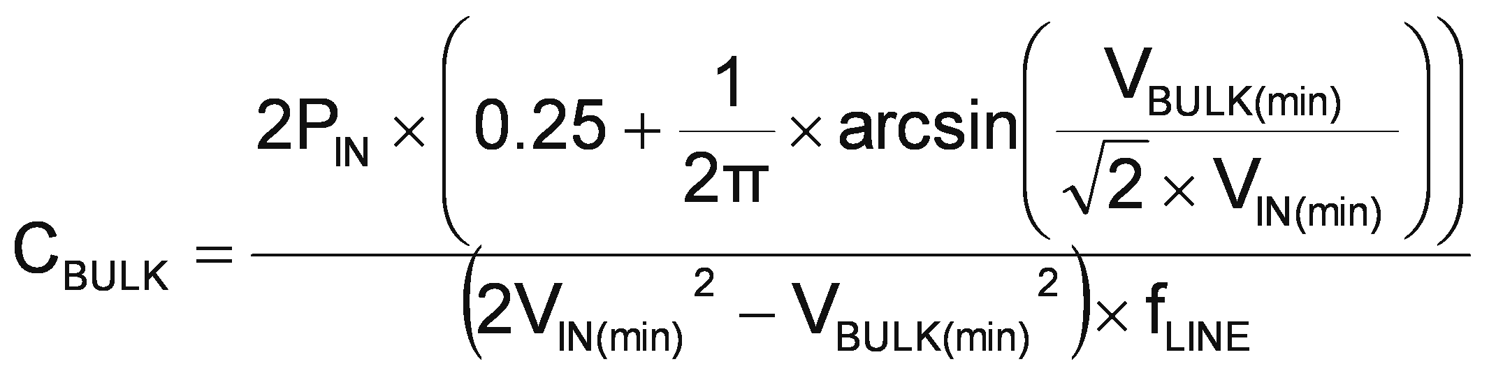
9.2.2.6 Input Bulk Capacitance and Minimum Bulk Voltage
Determine the minimum voltage on the input capacitance, CB1 and CB2 total, in order to determine the maximum Np to Ns turns ratio of the transformer. The input power of the converter based on target full-load efficiency, minimum input RMS voltage, and minimum AC input frequency are used to determine the input capacitance requirement.
Maximum input power is determined based on VOCV, IOCC, and the full-load efficiency target.
The below equation provides an accurate solution for input capacitance based on a target minimum bulk capacitor voltage. To target a given input capacitance value, iterate the minimum capacitor voltage to achieve the target capacitance.
9.2.2.7 Transformer Turns Ratio, Inductance, Primary-Peak Current
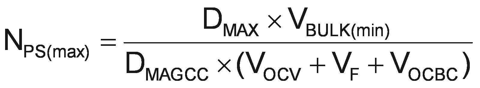
The maximum primary-to-secondary turns ratio can be determined by the target maximum switching frequency at full load, the minimum input capacitor bulk voltage, and the estimated DCM quasi-resonant time.
Initially determine the maximum available total duty cycle of the on time and secondary conduction time based on target switching frequency and DCM resonant time. For DCM resonant time, assume 500 kHz if you do not have an estimate from previous designs. For the transition mode operation limit, the period required from the end of secondary current conduction to the first valley of the VDS voltage is ½ of the DCM resonant period, or 1 µs assuming 500-kHz resonant frequency. DMAX can be determined using the equation below.
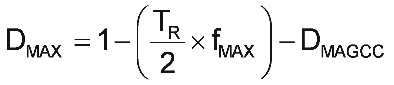
Once DMAX is known, the maximum turns ratio of the primary to secondary can be determined with the equation below. DMAGCC is defined as the secondary diode conduction duty cycle during constant-current, CC, operation. It is set internally by the UCC28700 at 0.425. The total voltage on the secondary winding needs to be determined; which is the sum of VOCV, the secondary rectifier VF, and the cable compensation voltage (VOCBC). For the 5-V USB charger applications, a turns ratio range of 13 to 15 is typically used.
Once an optimum turns ratio is determined from a detailed transformer design, use this ratio for the following parameters.
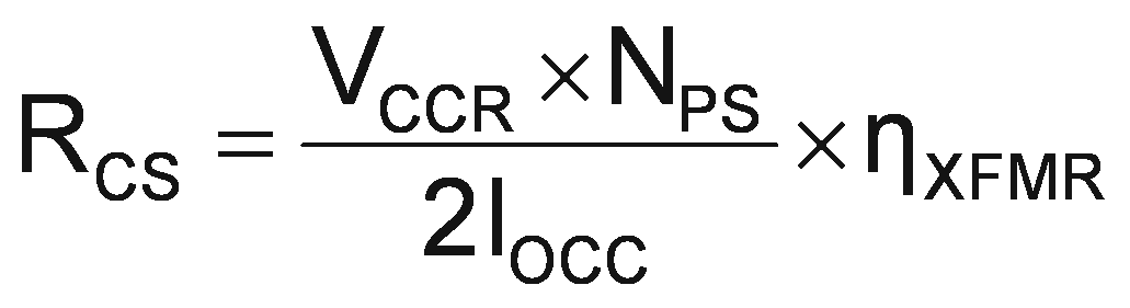
The UCC28700 controller constant-current regulation is achieved by maintaining a maximum DMAG duty cycle of 0.425 at the maximum primary current setting. The transformer turns ratio and constant-current regulating voltage determine the current sense resistor for a target constant current.
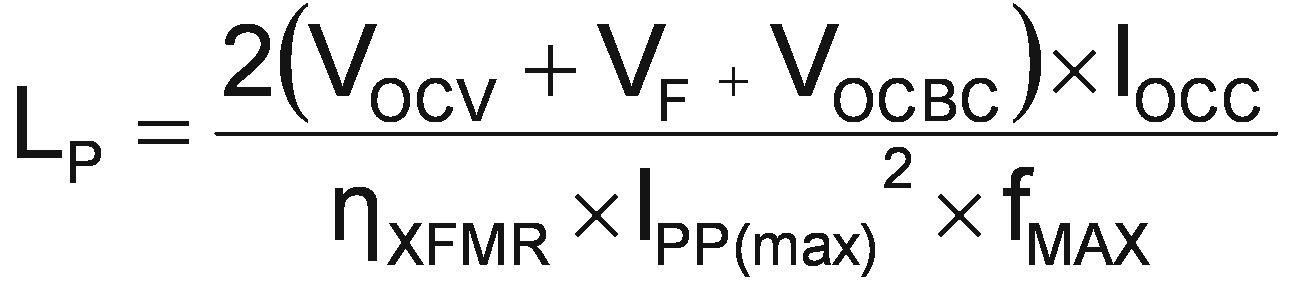
Since not all of the energy stored in the transformer is transferred to the secondary, a transformer efficiency term is included. This efficiency number includes the core and winding losses, leakage inductance ratio, and bias power ratio to rated output power. For a 5-V, 1-A charger example, bias power of 1.5% is a good estimate. An overall transformer efficiency of 0.9 is a good estimate to include 3.5% leakage inductance, 5% core and winding loss, and 1.5% bias power.
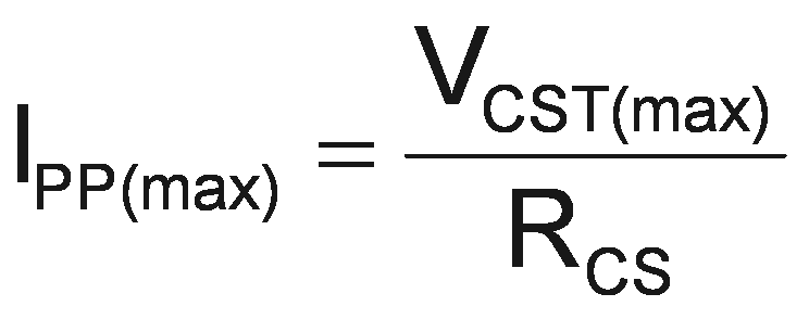
The primary transformer inductance can be calculated using the standard energy storage equation for flyback transformers. Primary current, maximum switching frequency and output and transformer power losses are included in the equation below. Initially determine transformer primary current.
Primary current is simply the maximum current sense threshold divided by the current sense resistance.
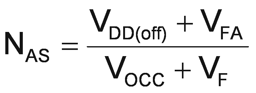
The secondary winding to auxiliary winding transformer turns ratio (NAS) is determined by the lowest target operating output voltage in constant-current regulation and the VDD UVLO of the UCC28700. There is additional energy supplied to VDD from the transformer leakage inductance energy which allows a lower turns ratio to be used in many designs.
9.2.2.8 Standby Power Estimate
Assuming no-load standby power is a critical design parameter, determine estimated no-load power based on target converter maximum switching frequency and output power rating.
The following equation estimates the stand-by power of the converter.

For a typical USB charger application, the bias power during no-load is approximately 2.5 mW. This is based on 25-V VDD and 100-µA bias current. The output preload resistor can be estimated by VOCV and the difference in the converter stand-by power and the bias power. The equation for output preload resistance accounts for bias power estimated at 2.5 mW.
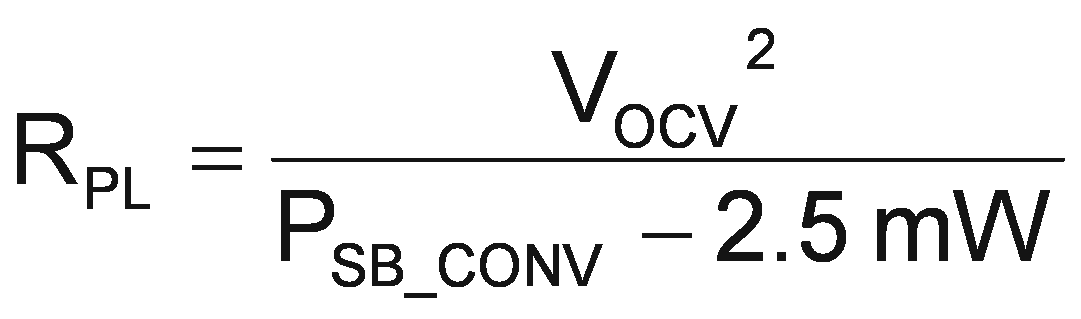
Typical start-up resistance values for RSTR range from 13 MΩ to 20 MΩ to achieve 1-s start-up time. The capacitor bulk voltage for the loss estimation is the highest voltage for the stand-by power measurement, typically 325 VDC.
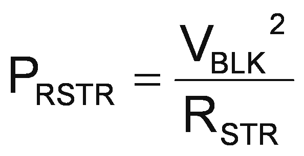
For the total stand-by power estimation add an estimated 2.5 mW for snubber loss to the start-up resistance and converter stand-by power loss.

9.2.3 Application Curves
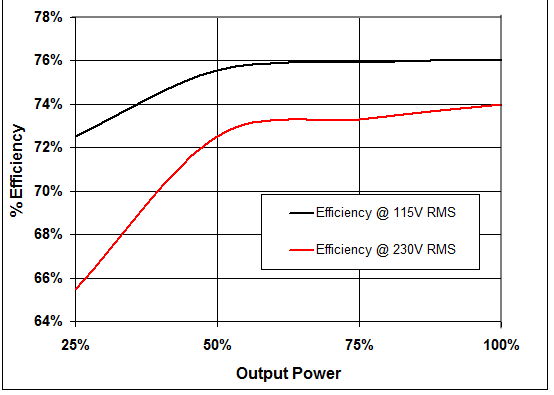 Figure 20. Efficiency
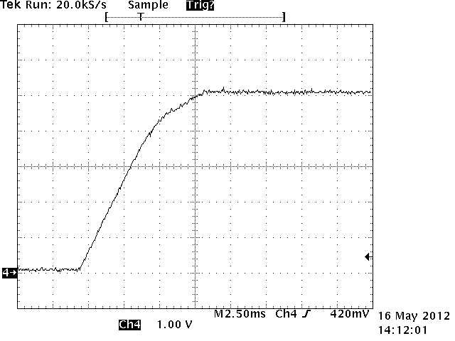 Figure 22. Output at Startup at 115-V RMS
(5-Ω Load)
(5-Ω Load)
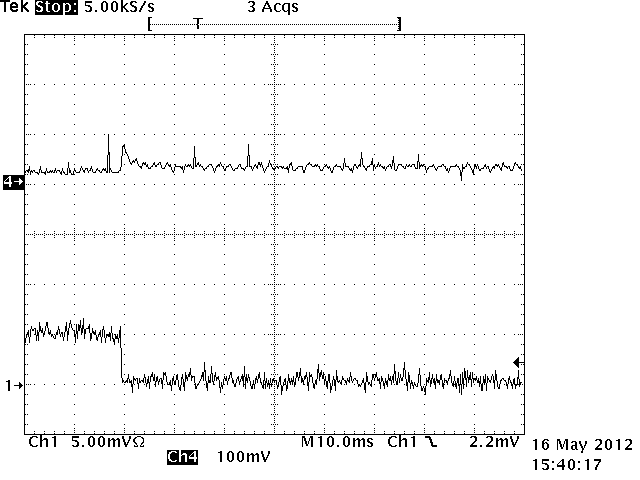
| CH1 = IO, CH4 = VO With a 5-V Offset | ||
(0.6-A to 0.1-A Load Step)
 Figure 21. Output at Startup at 115-V RMS
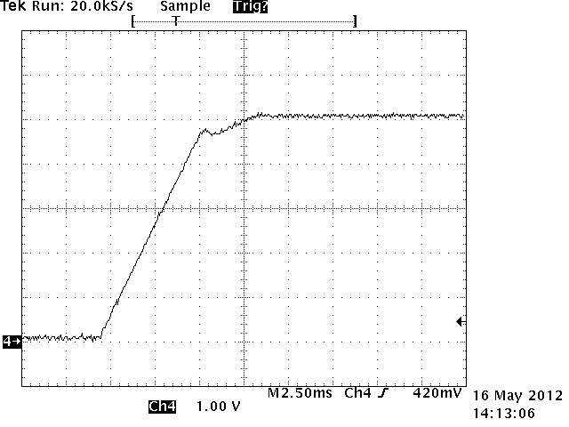
(No Load)
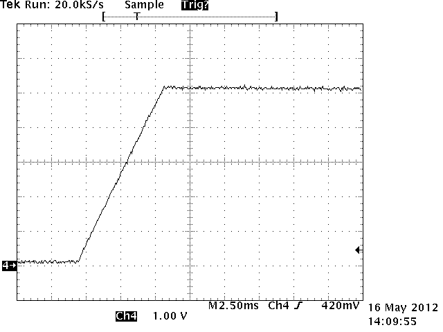 Figure 23. Output at Startup at 230-V RMS
(No Load)
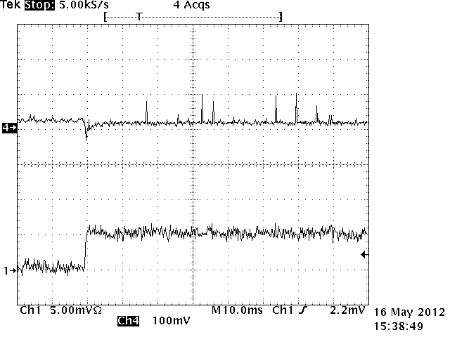
| CH1 = IO, CH4 = VO With a 5-V Offset |
(0.1-A to 0.6-A Load Step)
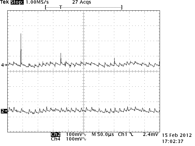
| CH4 = VO, Output voltage at EVM output | ||
| CH2 = VO, Output voltage measured at the end of the 3M of cable in parallel with a 1-uF capacitor. The output voltage has less than 50 mV of output ripple at the end of the cable. |