SLUS161G April 1999 – April 2025 UCC2813-0 , UCC2813-1 , UCC2813-2 , UCC2813-3 , UCC2813-4 , UCC2813-5 , UCC3813-0 , UCC3813-1 , UCC3813-2 , UCC3813-3 , UCC3813-4 , UCC3813-5
PRODUCTION DATA
- 1
- 1 Features
- 2 Applications
- 3 Description
- 4 Device Comparison Table
- 5 Pin Configuration and Functions
- 6 Specifications
-
7 Detailed Description
- 7.1 Overview
- 7.2 Functional Block Diagram
- 7.3
Feature Description
- 7.3.1 Detailed Pin Descriptions
- 7.3.2 Undervoltage Lockout (UVLO)
- 7.3.3 Self-Biasing, Active Low Output
- 7.3.4 Reference Voltage
- 7.3.5 Oscillator
- 7.3.6 Synchronization
- 7.3.7 PWM Generator
- 7.3.8 Minimum Off-Time Adjustment (Dead-Time Control)
- 7.3.9 Leading Edge Blanking
- 7.3.10 Minimum Pulse Width
- 7.3.11 Current Limiting
- 7.3.12 Overcurrent Protection and Full-Cycle Restart
- 7.3.13 Soft Start
- 7.3.14 Slope Compensation
- 7.4 Device Functional Modes
-
8 Application and Implementation
- 8.1 Application Information
- 8.2
Typical Application
- 8.2.1 Design Requirements
- 8.2.2
Detailed Design Procedure
- 8.2.2.1 Bulk Capacitor Calculation
- 8.2.2.2 Transformer Design
- 8.2.2.3 MOSFET and Output Diode Selection
- 8.2.2.4 Output Capacitor Calculation
- 8.2.2.5 Current Sensing Network
- 8.2.2.6 Gate Drive Resistor
- 8.2.2.7 REF Bypass Capacitor
- 8.2.2.8 RT and CT
- 8.2.2.9 Start-Up Circuit
- 8.2.2.10 Voltage Feedback Compensation Procedure
- 8.2.3 Application Curves
- 8.3 Power Supply Recommendations
- 8.4 Layout
- 9 Device and Documentation Support
- 10Revision History
- 11Mechanical, Packaging, and Orderable Information
Package Options
Refer to the PDF data sheet for device specific package drawings
Mechanical Data (Package|Pins)
- D|8
- PW|8
Thermal pad, mechanical data (Package|Pins)
Orderable Information
8.2.2.10.1 Power Stage Gain, Zeroes, and Poles
The first step in compensating a fixed-frequency flyback is to verify if the converter operates in continuous conduction mode (CCM) or discontinuous conduction mode (DCM). If the primary inductance (LP) is greater than the inductance for DCM-CCM boundary mode operation, called the critical inductance (LPcrit), then the converter operates in CCM. LPcrit is calculated with Equation 17.

For loads greater than 10% of PMAX over the entire input voltage range, the selected primary inductance has value larger than the critical inductance. Therefore, the converter operates in CCM and the compensation loop requires design based on CCM flyback equations.
The current-to-voltage conversion is done externally with the ground-referenced current-sense resistor (RCS) and the internal resistor divider sets up the internal current-sense gain, ACS = 1.65. The IC technology allows tight control of the resistor-divider ratio, regardless of the actual resistor value variations.
The DC open-loop gain (GO) of the fixed-frequency voltage control loop of a peak-current-mode control CCM flyback converter shown in Figure 8-1 is approximated by first using the output load (ROUT), the primary to secondary turns ratio (NPS), and the maximum duty cycle (D) as shown in Equation 18.
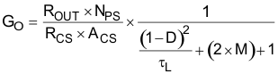
where
- ROUT = VOUT / IOUT
- D is calculated with Equation 19
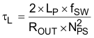
- τL is calculated with Equation 20
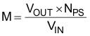
- M is calculated with Equation 21

For this design, a converter with an output voltage (VOUT) of 12 V, and 48 W relates to an output load (ROUT) equal to 3 Ω at full load.
At minimum input bulk voltage of 75 V DC, the duty cycle reaches its maximum value of 0.615. The current sense resistance (RCS) is 0.75 Ω and a primary to secondary turns-ratio (NPS) is 10. The open-loop gain calculates to 14.95 dB.
A CCM flyback transfer function has two zeroes that are of interest. The ESR and the output capacitance contribute a left-half plane zero to the power stage, and the frequency of this zero (fESRz) is calculated with Equation 22.

The fESRz zero for a capacitance bank of three 680-µF capacitors (for a total output capacitance of 2040 µF) and a total ESR of 13 mΩ is located at 6 kHz.
CCM flyback converters have a zero in the right-half plane (RHP) of their transfer function. RHP zero has the same 20 dB/decade rising gain magnitude with increasing frequency just like a left-half plane zero, but it adds phase lag instead of lead. This phase lag tends to limit the overall loop bandwidth. The frequency location (fRHPz) in Equation 23 is a function of the output load, the duty cycle, the primary inductance (LP), and the primary to secondary side turns ratio (NPS).
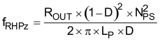
RHP zero frequency increases with higher input voltage and lighter load. Generally, the design requires consideration of the worst case of the lowest RHP zero frequency and the converter must be compensated at the minimum input and maximum load condition. With a primary inductance of 1.5 mH, at 75-V DC input, the RHP zero frequency (fRHPz) is equal to 7.65 kHz at maximum duty cycle (full load).
The power stage has one dominant pole (ωP1) which is in the region of interest, located at a lower frequency (fP1) which is related to the duty cycle (D), the output load, and the output capacitance. There is also a double pole (fP2) located at half the switching frequency of the converter. These poles are frequencies calculated with Equation 24 and Equation 25.


Subharmonic oscillation is the large signal instability that can occur in CCM flyback converters when duty cycles extend beyond 50%. The subharmonic oscillation increases the output voltage ripple and sometimes it even limits the power handling capability of the converter. Slope compensation to the CS signal is a technique used to eliminate the instability.
Ideally, the target of slope compensation is to achieve quality coefficient (QP = 1) at half of the switching frequency. The QP is calculated by Equation 26.

where
- D is the primary side switch duty cycle
- MC is the slope compensation factor, which is defined by Equation 27

where
- Se is the compensation ramp slope
- Sn represents the rising current slope of the transformer primary inductance
The optimal goal of the slope compensation is to achieve QP equal to 1, which means MC must be 2.128 when D reaches it maximum value of 0.615.
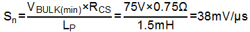
The inductance current slope at the CS pin is calculated by Equation 28.
The compensation slope is calculated by Equation 29.

The compensation slope is added into the system through RRAMP and RCSF. A series capacitor (CRAMP) is selected to approximate a high-frequency short circuit. Choose CRAMP as 10 nF as the starting point, and make adjustments if required. RRAMP and RCSF form a voltage divider to scale the RC pin ramp voltage and inject the slope compensation into CS pin. Choose RRAMP much larger than the RT resistor so that it does not affect the frequency setting very much. In this design, RRAMP is selected as 24.9 kΩ. The RC pin ramp slope is calculated with Equation 30.

To achieve 46.3 mV/µs compensation slope, RCSF resistor is calculated with Equation 31.

The power stage open-loop gain and phase can be plotted as a function of frequency. The total open-loop transfer function, as a function of frequency, can be characterized by Equation 32.

where
- ωP1 and ωP2 are based on the frequencies calculated by Equation 24 and Equation 25
The open-loop gain and phase Bode plots are graphed accordingly (see Figure 8-2 and Figure 8-3).
 Figure 8-2 Converter Open-Loop Bode Plot: Gain
 Figure 8-3 Converter Open-Loop Bode Plot: Phase