SLUS645F February 2005 – December 2014 UCD7201
PRODUCTION DATA.
- 1 Features
- 2 Applications
- 3 Description
- 4 Revision History
- 5 Description (Continued)
- 6 Pin Configuration and Functions
- 7 Specifications
- 8 Detailed Description
- 9 Applications and Implementation
- 10Power Supply Recommendations
- 11Layout
- 12Device and Documentation Support
- 13Mechanical, Packaging, and Orderable Information
Package Options
Mechanical Data (Package|Pins)
- PWP|14
Thermal pad, mechanical data (Package|Pins)
- PWP|14
Orderable Information
11 Layout
11.1 Layout Guidelines
In a power driver operating at high frequency, it is critical to minimize stray inductance to minimize overshoot/undershoots and ringing. The low output impedance of these drivers produces waveforms with high di/dt. This tends to induce ringing in the parasitic inductances. It is advantageous to connect the driver device close to the MOSFETs. It is recommended that the PGND and the AGND pins be connected to the PowerPad™ of the package with a thin trace. It is critical to ensure that the voltage potential between these two pins does not exceed 0.3 V. The use of schottky diodes on the outputs to PGND and PVDD is recommended when driving gate transformers.
11.2 Layout Example
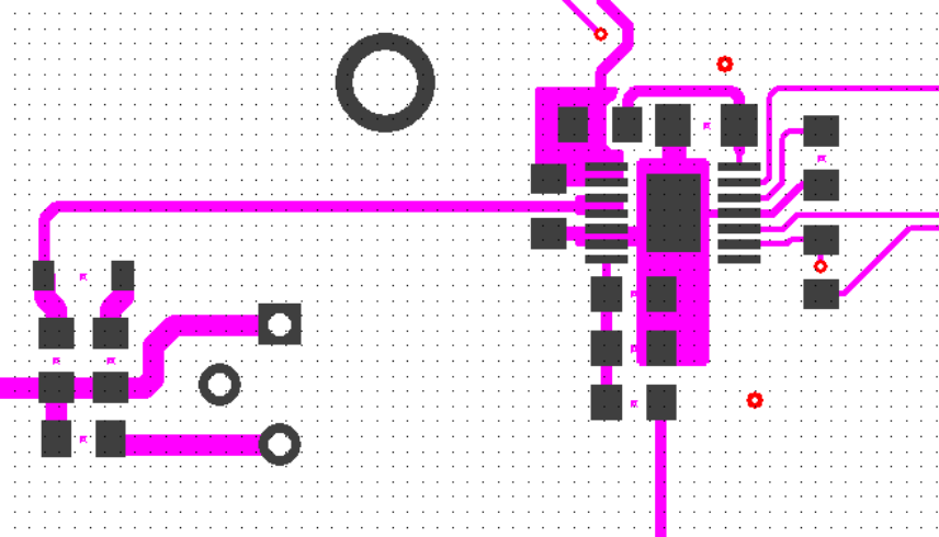 Figure 28. UCD7100 Layout Example
11.3 Thermal Considerations
The useful range of a driver is greatly affected by the drive power requirements of the load and the thermal characteristics of the device package. In order for a power driver to be useful over a particular temperature range the package must allow for the efficient removal of the heat produced while keeping the junction temperature within rated limits. The UCD7K family of drivers is available in PowerPAD™ TSSOP and QFN/DFN packages to cover a range of application requirements. Both have an exposed pad to enhance thermal conductivity from the semiconductor junction.
As illustrated in Reference [2], the PowerPAD™ packages offer a leadframe die pad that is exposed at the base of the package. This pad is soldered to the copper on the PC board (PCB) directly underneath the device package, reducing the TJC down to 2.07°C/W. The PC board must be designed with thermal lands and thermal vias to complete the heat removal subsystem, as summarized in Reference [3].
Note that the PowerPAD™ is not directly connected to any leads of the package. However, it is electrically and thermally connected to the substrate which is the ground of the device. The PowerPad™ should be connected to the quiet ground of the circuit.