SLUSB36C June 2012 – January 2015 UCD8220-Q1
PRODUCTION DATA.
- 1 Features
- 2 Applications
- 3 Description
- 4 Revision History
- 5 Pin Configuration and Functions
- 6 Specifications
- 7 Detailed Description
- 8 Application and Implementation
- 9 Power Supply Recommendations
- 10Layout
- 11Device and Documentation Support
- 12Mechanical, Packaging, and Orderable Information
Package Options
Mechanical Data (Package|Pins)
- PWP|16
Thermal pad, mechanical data (Package|Pins)
- PWP|16
Orderable Information
6 Specifications
6.1 Absolute Maximum Ratings(1)(2)
| MIN | MAX | UNIT | ||
|---|---|---|---|---|
| Supply voltage, VDD | 16 | V | ||
| Supply current, IDD | Quiescent | 20 | mA | |
| Switching, TA = 25°C, TJ = 125°C, VDD = 12 V | 200 | |||
| Output gate-drive voltage, VO | OUTx | –1 | PVDD | V |
| Output gate-drive sink current, IO(sink) | OUTx | 4 | A | |
| Output gate-drive source current, IO(source) | OUTx | –4 | ||
| Analog input | ISET, CS, CTRL, ILIM | –0.3 | 3.6 | V |
| Digital I/Os | CLK, CLF | –0.3 | 3.6 | |
| Continuous total power dissipation | See Thermal Information | |||
| Operating junction temperature range, TJ | –55 | 150 | °C | |
| Lead temperature (Soldering, 10 sec) | 300 | °C | ||
| Storage temperature, Tstg | –65 | 150 | °C | |
(1) Stresses beyond those listed under absolute maximum ratings may cause permanent damage to the device. These are stress ratings only, and functional operation of the device at these or any other conditions beyond those indicated under recommended operating conditions is not implied. Exposure to absolute-maximum-rated conditions for extended periods may affect device reliability.
(2) All voltages are with respect to GND. Currents are positive into, negative out of the specified terminal.
6.2 ESD Ratings
| VALUE | UNIT | ||||
|---|---|---|---|---|---|
| V(ESD) | Electrostatic discharge | Human body model (HBM), per AEC Q100-002(1) | ±2000 | V | |
| Charged device model (CDM), per AEC Q100-011 | Corner pins (1, 8, 9, and 16) | ±750 | |||
| Other pins | ±500 | ||||
(1) AEC Q100-002 indicates HBM stressing is done in accordance with the ANSI/ESDA/JEDEC JS-001 specification.
6.3 Recommended Operating Conditions
over operating free-air temperature range (unless otherwise noted)| MIN | MAX | UNIT | ||
|---|---|---|---|---|
| VDD | Supply voltage, PVDD | 4.5 | 15.5 | V |
6.4 Thermal Information
| THERMAL METRIC(1) | PWP (HTSSOP) | UNIT | |
|---|---|---|---|
| 16 PINS | |||
| RθJA | Junction-to-ambient thermal resistance | 40.1 | °C/W |
| RθJC(top) | Junction-to-case (top) thermal resistance | 29.5 | |
| RθJB | Junction-to-board thermal resistance | 24.2 | |
| ψJT | Junction-to-top characterization parameter | 1 | |
| ψJB | Junction-to-board characterization parameter | 24 | |
| RθJC(bot) | Junction-to-case (bottom) thermal resistance | 1.8 | |
(1) For more information about traditional and new thermal metrics, see the IC Package Thermal Metrics application report, SPRA953.
6.5 Electrical Characteristics
VDD = 12 V, 4.7-µF capacitor from VDD to AGND, 1 μF from PVDD to PGND, 0.22-µF capacitor from 3V3 to AGND, TA = TJ = –40°C to 125°C, (unless otherwise noted).| PARAMETER | TEST CONDITIONS | MIN | TYP | MAX | UNIT | ||
|---|---|---|---|---|---|---|---|
| SUPPLY SECTION | |||||||
| Supply current, OFF | VDD = 4.2 V | 300 | 500 | µA | |||
| Supply current, ON | Outputs not switching, CLK = low | 1.6 | 3 | mA | |||
| LOW VOLTAGE UNDERVOLTAGE LOCKOUT | |||||||
| VDD UVLO ON | 4.25 | 4.5 | 4.75 | V | |||
| VDD UVLO OFF | 4.05 | 4.25 | 4.45 | V | |||
| VDD UVLO hysteresis | 150 | 250 | 350 | mV | |||
| REFERENCE / EXTERNAL BIAS SUPPLY | |||||||
| 3V3 initial set point | TA = 25°C, ILOAD = 0 | 3.267 | 3.3 | 3.333 | V | ||
| 3V3 set point over temperature | 3.234 | 3.3 | 3.366 | V | |||
| 3V3 load regulation | ILOAD = 1 mA to 10 mA, VDD = 5 V | 1 | 6.6 | mV | |||
| 3V3 line regulation | VDD = 4.75 V to 12 V, ILOAD = 10 mA | 1 | 6.6 | mV | |||
| Short circuit current | VDD = 4.75 to 12 V | 9 | 20 | 35 | mA | ||
| 3V3 OK threshold, ON | 3.3 V rising | 2.9 | 3.0 | 3.1 | V | ||
| 3V3 OK threshold, OFF | 3.3 V falling | 2.7 | 2.8 | 2.9 | V | ||
| CLOCK INPUT (CLK) | |||||||
| VIT+ | HIGH, positive-going input threshold voltage | 1.65 | 2.08 | V | |||
| VIT– | LOW negative-going input threshold voltage | 1.16 | 1.5 | V | |||
| (VIT+) – (VIT–) | Input voltage hysteresis | 0.6 | 0.8 | V | |||
| Frequency | OUTx = 1 MHz | 2 | MHz | ||||
| SLOPE COMPENSATION (ISET) | |||||||
| ISET Voltage | VISET , 3V3 = 3.3 V, ±2% | 1.78 | 1.84 | 1.90 | V | ||
| m | VSLOPE (I-Mode) | RISET = 6.19 kΩ to AGND, CS = 0.25 V, CTRL = 2.5 V | 1.48 | 2.12 | 2.76 | V/µs | |
| RISET = 100 kΩ to AGND, CS = 0.25 V, CTRL = 2.5 V | 0.099 | 0.142 | 0.185 | ||||
| RISET = 499 kΩ to AGND, CS = 0.25 V, CTRL = 2.5 V | 0.019 | 0.028 | 0.037 | ||||
| m | VSLOPE (V-Mode) | RISET = 4.99 kΩ to 3V3, CTRL = 2.5 V | 1.44 | 2.06 | 2.68 | V/µs | |
| RISET = 100 kΩ to 3V3, CTRL = 2.5 V | 0.068 | 0.114 | 0.148 | ||||
| RISET = 402 kΩ to 3v3, CTRL = 2.5 V | 0.016 | 0.027 | 0.035 | ||||
| ISET resistor range | Current mode control; RISET connected to AGND | 6.19 | 499 | kΩ | |||
| ISET resistor range | Voltage mode control; RISET connected to 3V3 | 4.99 | 402 | kΩ | |||
| ISET current range | Voltage mode control with Feed-Forward; RISET connected to VIN | 3.7 | 300 | μA | |||
| PWM | |||||||
| PWM offset at CTRL input | 3V3 = 3.3 V ±2% | 0.45 | 0.51 | 0.6 | V | ||
| CTRL buffer gain(1) | Gain from CTRL to PWM comparator input | 0.5 | V/V | ||||
| CURRENT LIMIT (ILIM) | |||||||
| ILIM internal current limit threshold | ILIM = OPEN | 0.466 | 0.5 | 0.536 | V | ||
| ILIM maximum current limit threshold | ILIM = 3.3 V | 0.975 | 1.025 | 1.075 | V | ||
| ILIM current limit threshold | ILIM = 0.75 V | 0.700 | 0.725 | 0.750 | V | ||
| ILIM minimum current limit threshold | ILIM = 0.25 V | 0.2 | 0.23 | 0.25 | V | ||
| CLF output high level | CS > ILIM , ILOAD = –7 mA | 2.64 | V | ||||
| CLF output low level | CS ≤ ILIM, ILOAD = 7 mA | 0.66 | V | ||||
| CURRENT SENSE COMPARATOR | |||||||
| Bias voltage | Includes CS comp offset | 5 | 25 | 50 | mV | ||
| Input bias current | –1 | μA | |||||
| CURRENT SENSE DISCHARGE TRANSISTOR | |||||||
| Discharge resistance | CLK = low, resistance from CS to AGND | 10 | 35 | 75 | Ω | ||
| OUTPUT DRIVERS | |||||||
| Source current(1) | VDD = 12 V, CLK = high, OUTx = 5 V | 4 | A | ||||
| Sink current(1) | VDD = 12 V, CLK = low, OUTx = 5 V | 4 | A | ||||
| Source current(1) | VDD = 4.75 V, CLK = high, OUTx = 0 | 2 | A | ||||
| Sink current(1) | VDD = 4.75 V, CLK = low, OUTx = 4.75 V | 3 | A | ||||
| Output with VDD < UVLO | VDD = 1.0 V, ISINK = 10 mA | 0.8 | 1.2 | V | |||
(1) Specified by design. Not 100% tested in production.
6.6 Timing Requirements
VDD = 12 V, 4.7-µF capacitor from VDD to AGND, 1 μF from PVDD to PGND, 0.22-µF capacitor from 3V3 to AGND, TA = TJ = –40°C to 125°C, (unless otherwise noted).| MIN | NOM | MAX | UNIT | |||
|---|---|---|---|---|---|---|
| CLOCK INPUT (CLK) | ||||||
| Minimum allowable off time(1) | 20 | ns | ||||
| CURRENT LIMIT (ILIM) | ||||||
| Propagation delay from CLK to CLF | CLK rising to CLF falling after a current limit event | 15 | 25 | ns | ||
| CURRENT SENSE COMPARATOR | ||||||
| Propagation delay from CS to OUTx | ILIM = 0.5 V, measured on OUTx, CS = threshold + 60 mV | 25 | 40 | ns | ||
| Propagation delay from CS to CLF | ILIM = 0.5 V, measured on CLF, CS = threshold + 60 mV | 25 | 50 | |||
| OUTPUT DRIVERS | ||||||
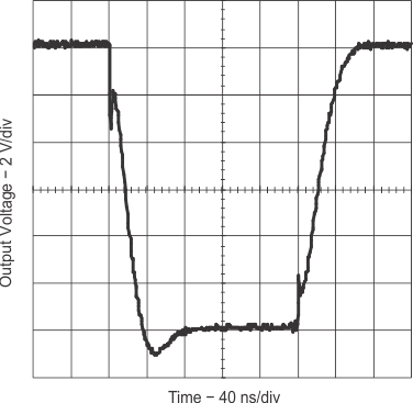
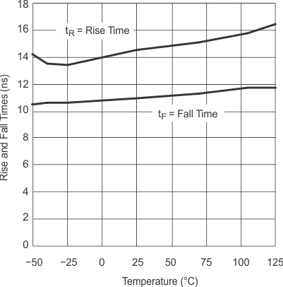
| tR | Rise time | CLOAD = 2.2 nF, VDD = 12 V, See Figure 1 | 10 | 20 | ns | |
| tF | Fall time | CLOAD = 2.2 nF, VDD = 12 V, See Figure 1 | 10 | 15 | ||
| tD1 | Propagation delay from CLK to OUTx, CLK rising | CLOAD = open, VDD = 12 V, See Figure 1 | 25 | 35 | ns | |
| tD2 | Propagation delay from CLK to OUTx, CLK falling | CLOAD = open, VDD = 12 V, See Figure 1 | 25 | 35 | ||
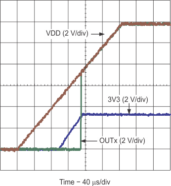
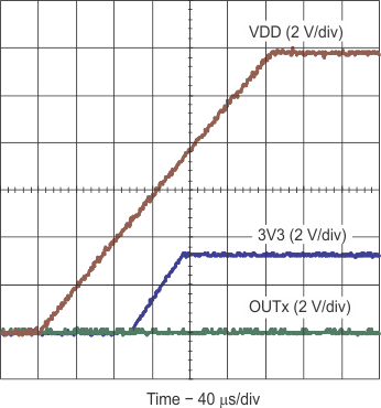
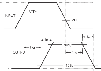 Figure 1. Timing Diagram
6.7 Typical Characteristics
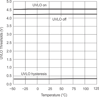 Figure 2. UCD8220-Q1 UVLO Threshold vs Temperature
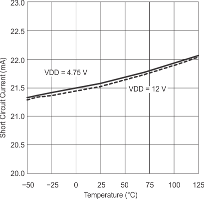 Figure 4. 3V3 Short-circuit Current vs Temperature
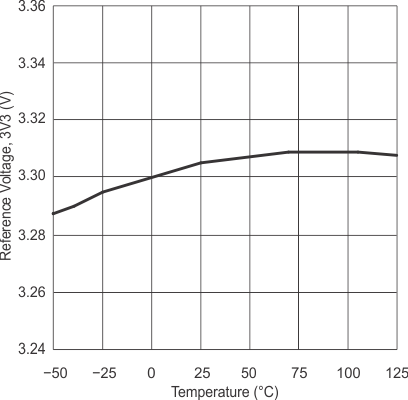 Figure 3. 3V3 Reference Voltage vs Temperature
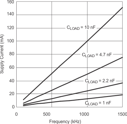 Figure 5. Supply Current vs Frequency (VDD = 5 V)
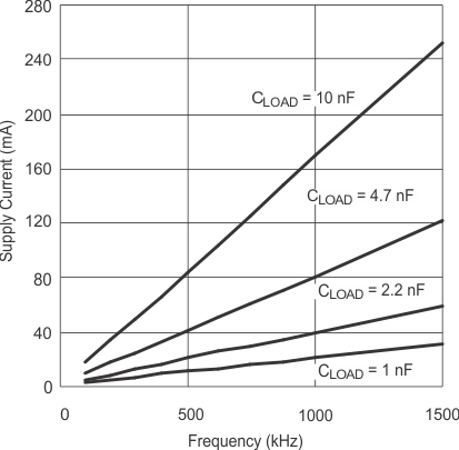 Figure 6. Supply Current vs Frequency (VDD = 8 V)
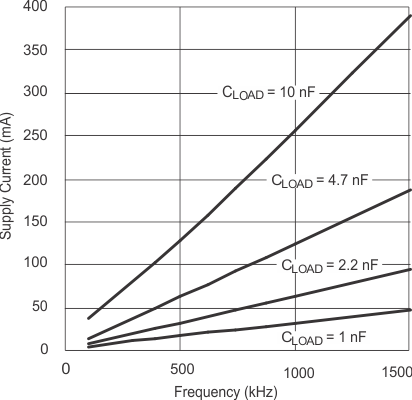 Figure 8. Supply Current vs Frequency (VDD = 12 V)
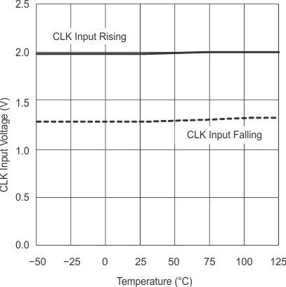
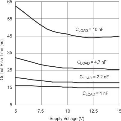
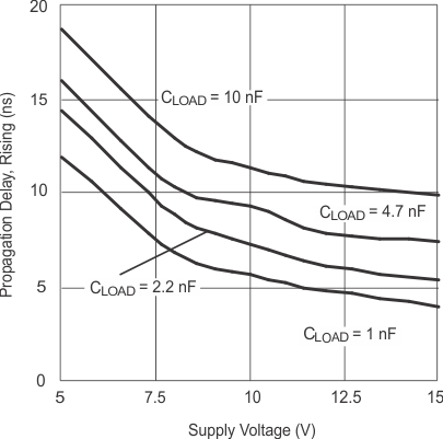 Figure 14. CLK to OUTx Propagation Delay Rising vs Supply Voltage
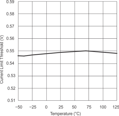 Figure 16. Default Current Limit Threshold vs Temperature
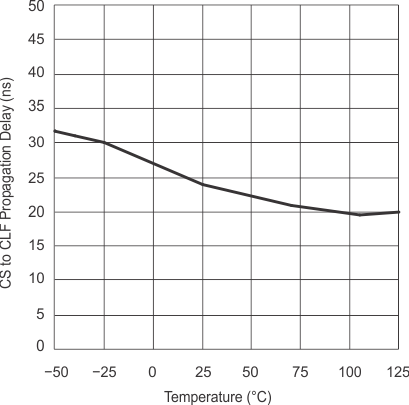 Figure 18. CS to CLF Propagation Delay vs Temperature
| CLK = CTRL = 3V3 |
| CLK = AGND | CTRL = 3V3 |
| VDD = 12 V | CLOAD = 10 nF |
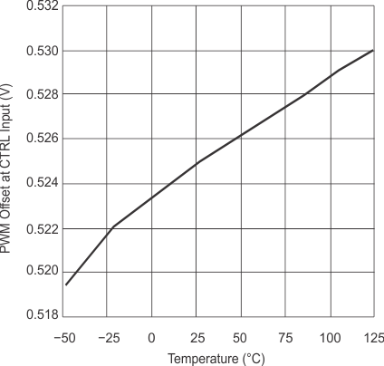
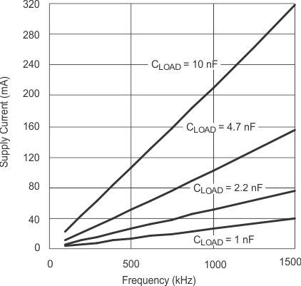 Figure 7. Supply Current vs Frequency (VDD = 10 V)
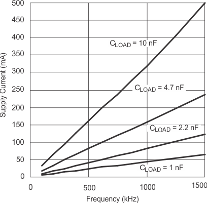 Figure 9. Supply Current vs Frequency (VDD = 15 V)
| CLOAD = 2.2 nF | VDD = 12 V |
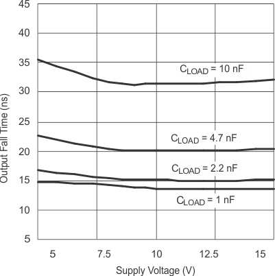
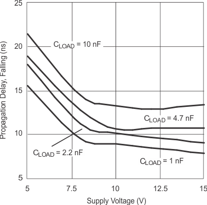 Figure 15. CLK to OUTx Propagation Delay Falling vs Supply Current
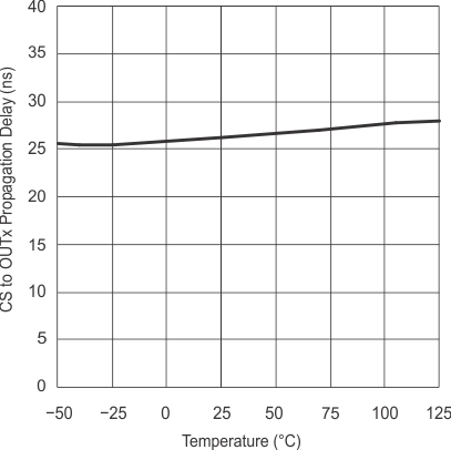 Figure 17. CS to OUTx Propagation Delay vs Temperature
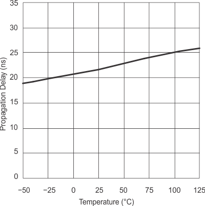 Figure 19. CLK to OUT Propagation Delay vs Temperature
| CLK = CTRL = 3V3 |
| CLK = AGND | CTRL = 3V3 |
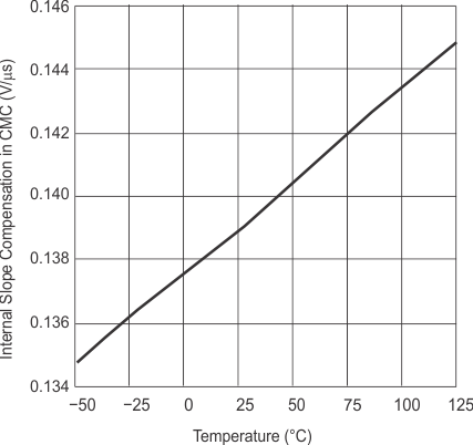
| Current mode slope | RISET = 100 kΩ |