SLVSAN9C April 2011 – March 2019 UCD90120A
PRODUCTION DATA.
- 1 Features
- 2 Applications
- 3 Description
- 4 Revision History
- 5 Pin Configuration and Functions
- 6 Specifications
-
7 Detailed Description
- 7.1 Overview
- 7.2 Functional Block Diagram
- 7.3 Feature Description
- 7.4
Device Functional Modes
- 7.4.1 Power-Supply Sequencing
- 7.4.2 Pin-Selected Rail States
- 7.4.3 Monitoring
- 7.4.4 Fault Responses and Alert Processing
- 7.4.5 Shut Down All Rails and Sequence On (Resequence)
- 7.4.6 GPIOs
- 7.4.7 GPO Control
- 7.4.8 GPO Dependencies
- 7.4.9 GPO Delays
- 7.4.10 State Machine Mode Enable
- 7.4.11 GPI Special Functions
- 7.4.12 Power-Supply Enables
- 7.4.13 Cascading Multiple Devices
- 7.4.14 PWM Outputs
- 7.4.15 Programmable Multiphase PWMs
- 7.4.16 Margining
- 7.4.17 System Reset Signal
- 7.4.18 Watch Dog Timer
- 7.4.19 Run Time Clock
- 7.4.20 Data and Error Logging to Flash Memory
- 7.4.21 Brownout Function
- 7.4.22 PMBus Address Selection
- 7.5 Programming
- 8 Application and Implementation
- 9 Power Supply Recommendations
- 10Layout
- 11Device and Documentation Support
- 12Mechanical, Packaging, and Orderable Information
Package Options
Mechanical Data (Package|Pins)
- RGC|64
Thermal pad, mechanical data (Package|Pins)
- RGC|64
Orderable Information
5 Pin Configuration and Functions
NOTE
The maximum number of configurable rails is 12. The maximum number of configurable GPIs is 8. The maximum number of configurable Boolean Logic GPOs is 12.
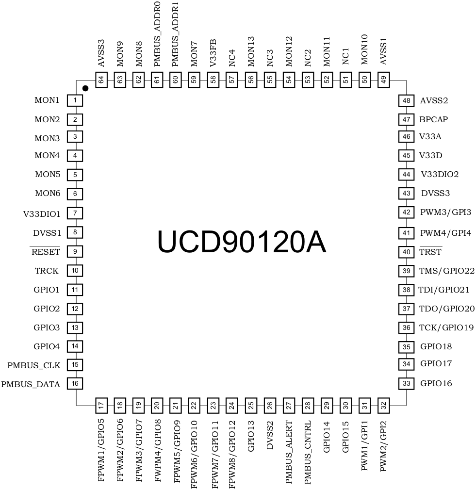
RGC Package
64-Pin VQFN
Top View

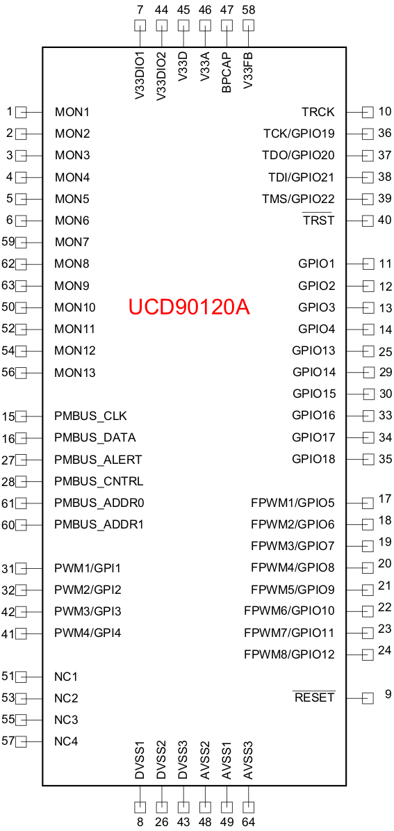
Simplified Pinout View

Pin Functions
| PIN | I/O TYPE | DESCRIPTION | ||
|---|---|---|---|---|
| NAME | NO. | |||
| ANALOG MONITOR INPUTS | ||||
| MON1 | 1 | I | Analog input (0 V–2.5 V) | |
| MON2 | 2 | I | Analog input (0 V–2.5 V) | |
| MON3 | 3 | I | Analog input (0 V–2.5 V) | |
| MON4 | 4 | I | Analog input (0 V–2.5 V) | |
| MON5 | 5 | I | Analog input (0 V–2.5 V) | |
| MON6 | 6 | I | Analog input (0 V–2.5 V) | |
| MON7 | 59 | I | Analog input (0 V–2.5 V) | |
| MON8 | 62 | I | Analog input (0 V–2.5 V) | |
| MON9 | 63 | I | Analog input (0 V–2.5 V) | |
| MON10 | 50 | I | Analog input (0.2 V–2.5 V) | |
| MON11 | 52 | I | Analog input (0.2 V–2.5 V) | |
| MON12 | 54 | I | Analog input (0.2 V–2.5 V) | |
| MON13 | 56 | I | Analog input (0.2 V–2.5 V) | |
| GPIO | ||||
| GPIO1 | 11 | I/O | General-purpose discrete I/O | |
| GPIO2 | 12 | I/O | General-purpose discrete I/O | |
| GPIO3 | 13 | I/O | General-purpose discrete I/O | |
| GPIO4 | 14 | I/O | General-purpose discrete I/O | |
| GPIO13 | 25 | I/O | General-purpose discrete I/O | |
| GPIO14 | 29 | I/O | General-purpose discrete I/O | |
| GPIO15 | 30 | I/O | General-purpose discrete I/O | |
| GPIO16 | 33 | I/O | General-purpose discrete I/O | |
| GPIO17 | 34 | I/O | General-purpose discrete I/O | |
| GPIO18 | 35 | I/O | General-purpose discrete I/O | |
| PWM OUTPUTS | ||||
| FPWM1/GPIO5 | 17 | I/O/PWM | PWM (15.259 kHz to 125 MHz) or GPIO | |
| FPWM2/GPIO6 | 18 | I/O/PWM | PWM (15.259 kHz to 125 MHz) or GPIO | |
| FPWM3/GPIO7 | 19 | I/O/PWM | PWM (15.259 kHz to 125 MHz) or GPIO | |
| FPWM4/GPIO8 | 20 | I/O/PWM | PWM (15.259 kHz to 125 MHz) or GPIO | |
| FPWM5/GPIO9 | 21 | I/O/PWM | PWM (15.259 kHz to 125 MHz) or GPIO | |
| FPWM6/GPIO10 | 22 | I/O/PWM | PWM (15.259 kHz to 125 MHz) or GPIO | |
| FPWM7/GPIO11 | 23 | I/O/PWM | PWM (15.259 kHz to 125 MHz) or GPIO | |
| FPWM8/GPIO12 | 24 | I/O/PWM | PWM (15.259 kHz to 125 MHz) or GPIO | |
| PWM1/GPI1 | 31 | I/PWM | Fixed 10-kHz PWM output or GPI | |
| PWM2/GPI2 | 32 | I/PWM | Fixed 1-kHz PWM output or GPI | |
| PWM3/GPI3 | 42 | I/PWM | PWM (0.93 Hz to 7.8125 MHz) or GPI | |
| PWM4/GPI4 | 41 | I/PWM | PWM (0.93 Hz to 7.8125 MHz) or GPI | |
| PMBus COMM INTERFACE | ||||
| PMBUS_CLK | 15 | I/O | PMBus clock (must have pullup to 3.3 V) | |
| PMBUS_DATA | 16 | I/O | PMBus data (must have pullup to 3.3 V) | |
| PMBALERT# | 27 | O | PMBus alert, active-low, open-drain output (must have pullup to 3.3 V) | |
| PMBUS_CNTRL | 28 | I | PMBus control | |
| PMBUS_ADDR0 | 61 | I | PMBus analog address input. Least-significant address bit | |
| PMBUS_ADDR1 | 60 | I | PMBus analog address input. Most-significant address bit | |
| JTAG | ||||
| TRCK | 10 | O | Test return clock | |
| TCK/GPIO19 | 36 | I/O | Test clock or GPIO | |
| TDO/GPIO20 | 37 | I/O | Test data out or GPIO | |
| TDI/GPIO21 | 38 | I/O | Test data in (tie to Vdd with 10-kΩ resistor) or GPIO | |
| TMS/GPIO22 | 39 | I/O | Test mode select (tie to Vdd with 10-kΩ resistor) or GPIO | |
| TRST | 40 | I | Test reset – tie to ground with 10-kΩ resistor | |
| INPUT POWER AND GROUNDS | ||||
| RESET | 9 | Active-low device reset input. Hold low for at least 2 μs to reset the device. | ||
| V33FB | 58 | Linear Regulator Feedback connection. Leave unconnected. | ||
| V33A | 46 | Analog 3.3-V supply. | Refer to the Layout Guidelines section. | |
| V33D | 45 | Digital core 3.3-V supply. | ||
| V33DIO1 | 7 | Digital I/O 3.3-V supply. | ||
| V33DIO2 | 44 | Digital I/O 3.3-V supply. | ||
| BPCap | 47 | 1.8-V bypass capacitor. | ||
| AVSS1 | 49 | Analog ground | ||
| AVSS2 | 48 | Analog ground | ||
| AVSS3 | 64 | Analog ground | ||
| DVSS1 | 8 | Digital ground | ||
| DVSS2 | 26 | Digital ground | ||
| DVSS3 | 43 | Digital ground | ||
| QFP ground pad | NA | Thermal pad – tie to ground plane. | ||