SNAS466G February 2009 – December 2016 ADC10D1000QML-SP
PRODUCTION DATA.
- 1 Features
- 2 Applications
- 3 Description
- 4 Revision History
- 5 Pin Configuration and Functions
-
6 Specifications
- 6.1 Absolute Maximum Ratings
- 6.2 ESD Ratings
- 6.3 Recommended Operating Conditions
- 6.4 Thermal Information
- 6.5 Converter Electrical Characteristics: Static Converter Characteristics
- 6.6 Converter Electrical Characteristics: Dynamic Converter Characteristics
- 6.7 Converter Electrical Characteristics: Analog Input/Output and Reference Characteristics
- 6.8 Converter Electrical Characteristics: Channel-to-Channel Characteristics
- 6.9 Converter Electrical Characteristics: LVDS CLK Input Characteristics
- 6.10 Electrical Characteristics: AutoSync Feature
- 6.11 Converter Electrical Characteristics: Digital Control and Output Pin Characteristics
- 6.12 Converter Electrical Characteristics: Power Supply Characteristics (1:2 Demux Mode)
- 6.13 Converter Electrical Characteristics: AC Electrical Characteristics
- 6.14 Timing Requirements: Serial Port Interface
- 6.15 Timing Requirements: Calibration
- 6.16 Quality Conformance Inspection
- 6.17 Timing Diagrams
- 6.18 Typical Characteristics
-
7 Detailed Description
- 7.1 Overview
- 7.2 Functional Block Diagram
- 7.3 Feature Description
- 7.4
Device Functional Modes
- 7.4.1
Control Modes
- 7.4.1.1
Non-Extended Control Mode
- 7.4.1.1.1 Non-Demultiplexed Mode Pin (NDM)
- 7.4.1.1.2 Dual Data-Rate Phase Pin (DDRPh)
- 7.4.1.1.3 Calibration Pin (CAL)
- 7.4.1.1.4 Power-Down I-Channel Pin (PDI)
- 7.4.1.1.5 Power-Down Q-Channel Pin (PDQ)
- 7.4.1.1.6 Test Pattern Mode Pin (TPM)
- 7.4.1.1.7 Full-Scale Input Range Pin (FSR)
- 7.4.1.1.8 AC-DC-Coupled Mode Pin (VCMO)
- 7.4.1.1.9 LVDS Output Common-Mode Pin (VBG)
- 7.4.1.1
Non-Extended Control Mode
- 7.4.2 Extended Control Mode
- 7.4.1
Control Modes
- 7.5 Programming
- 7.6 Register Maps
- 8 Application and Implementation
- 9 Power Supply Recommendations
- 10Layout
- 11Device and Documentation Support
- 12Mechanical, Packaging, and Orderable Information
Package Options
Refer to the PDF data sheet for device specific package drawings
Mechanical Data (Package|Pins)
- NAA|376
Thermal pad, mechanical data (Package|Pins)
Orderable Information
1 Features
- Space Qualified
- Total Ionizing Dose 100 krad(Si)
- Single-Event Latch-Up 120 MeV-cm2/mg
- Single-Event Functional-Interrupt Immune 120 MeV-cm2/mg (see Radiation Reports)
- Configurable to Either 1-GSPS Dual ADC or 2-GSPS Interleaved
- Low Power Consumption
- R/W SPI Interface for Extended Control Mode±
- Internally Terminated, Buffered, Differential Analog Inputs
- Test Patterns at Output for System Debug
- Programmable 15-Bit Gain and 12-Bit Plus Sign Offset Adjustments
- Option of 1:2 Demuxed or 1:1 Non-Demuxed LVDS Outputs
- Auto-Sync Feature for Multi-Chip Systems
- Single 1.9-V Power Supply
- Thermally Enhanced Column-Grid-Array Package
2 Applications
- Wideband Communications
- Direct RF Down Conversion
- Star Tracker
3 Description
The ADC10D1000 is a 10-bit, low-power, high-performance CMOS analog-to-digital converter (ADC) with sampling rates of up to 1 GSPS in dual-channel mode or 2 GSPS in single-channel mode. The ADC10D1000 achieves excellent accuracy and dynamic performance while consuming a typical 2.9 W of power.
The ADC10D1000 provides a flexible LVDS interface, which has multiple SPI-programmable options to facilitate board design and FPGA/ASIC data capture. The LVDS outputs are compatible with IEEE 1596.3- 1996 and support programmable common-mode voltage.
The product is packaged in a hermatic 376-pin column grid array (CCGA) that is thermally enhanced and rated over the temperature range of –55°C to +125°C.
Device Information(1)
| PART NUMBER | GRADE | PACKAGE |
|---|---|---|
| ADC10D1000CCMLS | Flight part 100 krad | CCGA (376) |
| ADC10D1000CCMPR | Pre-flight engineering prototype | CCGA (376) |
| ADC10D1000CVAL | Ceramic evaluation board | |
| ADC10D1000DAISY | Daisy chain, mechanical sample, no die | CCGA (376) |
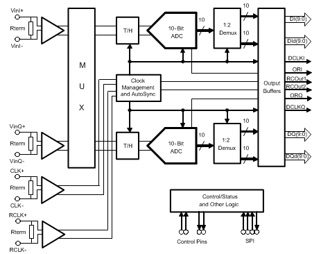
Functional Block Diagram
