SBAS561C June 2012 – January 2017 ADS131E04 , ADS131E06 , ADS131E08
PRODUCTION DATA.
- 1 Features
- 2 Applications
- 3 Description
- 4 Revision History
- 5 Device Comparison
- 6 Pin Configuration and Functions
- 7 Specifications
- 8 Parameter Measurement Information
-
9 Detailed Description
- 9.1 Overview
- 9.2 Functional Block Diagram
- 9.3 Feature Description
- 9.4 Device Functional Modes
- 9.5
Programming
- 9.5.1 Data Format
- 9.5.2 SPI Interface
- 9.5.3
SPI Command Definitions
- 9.5.3.1 Sending Multibyte Commands
- 9.5.3.2 WAKEUP: Exit STANDBY Mode
- 9.5.3.3 STANDBY: Enter STANDBY Mode
- 9.5.3.4 RESET: Reset Registers to Default Values
- 9.5.3.5 START: Start Conversions
- 9.5.3.6 STOP: Stop Conversions
- 9.5.3.7 OFFSETCAL: Channel Offset Calibration
- 9.5.3.8 RDATAC: Start Read Data Continuous Mode
- 9.5.3.9 SDATAC: Stop Read Data Continuous Mode
- 9.5.3.10 RDATA: Read Data
- 9.5.3.11 RREG: Read from Register
- 9.5.3.12 WREG: Write to Register
- 9.6
Register Map
- 9.6.1
Register Descriptions
- 9.6.1.1 ID: ID Control Register (Factory-Programmed, Read-Only) (address = 00h) [reset = xxh]
- 9.6.1.2 CONFIG1: Configuration Register 1 (address = 01h) [reset = 91h]
- 9.6.1.3 CONFIG2: Configuration Register 2 (address = 02h) [reset = E0h]
- 9.6.1.4 CONFIG3: Configuration Register 3 (address = 03h) [reset = 40]
- 9.6.1.5 FAULT: Fault Detect Control Register (address = 04h) [reset = 00h]
- 9.6.1.6 CHnSET: Individual Channel Settings (address = 05h to 0Ch) [reset = 10h]
- 9.6.1.7 FAULT_STATP: Fault Detect Positive Input Status (address = 12h) [reset = 00h]
- 9.6.1.8 FAULT_STATN: Fault Detect Negative Input Status (address = 13h) [reset = 00h]
- 9.6.1.9 GPIO: General-Purpose IO Register (address = 14h) [reset = 0Fh]
- 9.6.1
Register Descriptions
- 10Application and Implementation
- 11Power Supply Recommendations
- 12Layout
- 13Device and Documentation Support
- 14Mechanical, Packaging, and Orderable Information
Package Options
Mechanical Data (Package|Pins)
- PAG|64
Thermal pad, mechanical data (Package|Pins)
- PAG|64
Orderable Information
1 Features
- Eight Differential ADC Inputs
- Outstanding Performance:
- Dynamic Range: 118 dB at 1 kSPS
- Crosstalk: –110 dB
- THD: –90 dB at 50 Hz and 60 Hz
- Analog Supply Range Options:
- Digital: 1.8 V to 3.6 V
- Low Power: 2 mW per Channel
- Data Rates: 1, 2, 4, 8, 16, 32, and 64 kSPS
- Programmable Gains: 1, 2, 4, 8, and 12
- Fault Detection and Device Testing Capability
- SPI™ Data Interface and Four GPIOs
- Package: TQFP-64 (PAG)
- Operating Temperature Range:
–40°C to +105°C
2 Applications
- Power Protection: Circuit Breakers, and Relay Protection
- Energy Metering: Single Phase, Polyphase, and Power Quality
- Battery Test Systems
- Test and Measurement
- Simultaneous Sampling Data Acquisition Systems
3 Description
The ADS131E0x are a family of multichannel, simultaneous sampling, 24-bit, delta-sigma (ΔΣ), analog-to-digital converters (ADCs) with a built-in programmable gain amplifier (PGA), internal reference, and an onboard oscillator. The ADC wide dynamic range, scalable data rates, and internal fault detect monitors make the ADS131E0x attractive in industrial power monitoring and protection as well as test and measurement applications. True high-impedance inputs enable the ADS131E0x to directly interface with a resistor-divider network or a voltage transformer to measure line voltage, or a current transformer or Rogowski coil to measure line current. With high integration levels and exceptional performance, the ADS131E0x family enables the creation of scalable industrial power systems at significantly reduced size, power, and low overall cost.
The ADS131E0x have a flexible input multiplexer per channel that can be independently connected to the internally-generated signals for test, temperature, and fault detection. Fault detection can be implemented internal to the device, using the integrated comparators with digital-to-analog converter (DAC)-controlled trigger levels. The ADS131E0x can operate at data rates as high as 64 kSPS.
These complete analog front-end (AFE) solutions are packaged in a TQFP-64 package and are specified over the industrial temperature range of –40°C to +105°C.
Device Information(1)
| PART NUMBER | PACKAGE | BODY SIZE (NOM) |
|---|---|---|
| ADS131E0x | TQFP (64) | 10.00 mm × 10.00 mm |
- For all available packages, see the orderable addendum at the end of the data sheet.
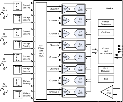
ADS131E08 Simplified Schematic

4 Revision History
Changes from B Revision (December 2013) to C Revision
- Added ESD Ratings table, Feature Description section, Device Functional Modes, Application and Implementation section, Power Supply Recommendations section, Layout section, Device and Documentation Support section, and Mechanical, Packaging, and Orderable Information section Go
- Changed formatting of Thermal Information table note Go
Changes from A Revision (April 2013) to B Revision
- Deleted device graphicGo
- Changed ADS131E0x family description to 24-bits only throughout documentGo
- Added AVSS to DGND row to Absolute Maximum Ratings tableGo
- Changed minimum specification to External Reference, VREFP parameter in Electrical Characteristics tableGo
- Changed conditions in Figure 10Go
- Changed conditions in Figure 11Go
- Changed START Opcode to START in Figure 39Go
- Changed Reset (RESET) section for clarityGo
- Changed Power-Up Sequencing sectionGo
Changes from * Revision (June 2012) to A Revision
- Deleted AGND to DGND row from Absolute Maximum Ratings tableGo
- Changed value of Digital input to DVDD row in Absolute Maximum Ratings tableGo
- Added minimum and maximum specifications to External Reference, Reference input voltage parameter in Electrical Characteristics tableGo
- Added minimum and maximum specifications to External Reference, VREFP parameter in Electrical Characteristics tableGo
- Changed Channel Performance (AC Performance), Accuracy parameter in Electrical Characteristics tableGo
- Changed Internal Reference, VO parameter in Electrical Characteristics tableGo
- Changed Internal Reference, Temperature drift parameter in Electrical Characteristics tableGo
- Added Figure 15 Go