SBAS652A May 2014 – August 2014 ADS7950-Q1 , ADS7951-Q1 , ADS7952-Q1 , ADS7953-Q1 , ADS7954-Q1 , ADS7956-Q1 , ADS7957-Q1 , ADS7958-Q1 , ADS7959-Q1 , ADS7960-Q1 , ADS7961-Q1
PRODUCTION DATA.
- 1 Features
- 2 Applications
- 3 Description
- 4 Revision History
- 5 Device Comparison Table
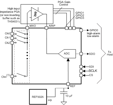
- 6 Pin Configurations and Functions
-
7 Specifications
- 7.1 Absolute Maximum Ratings
- 7.2 Handling Ratings
- 7.3 Recommended Operating Conditions
- 7.4 Thermal Information
- 7.5 Electrical Characteristics: ADS7950-Q1, ADS7951-Q1, ADS7952-Q1, ADS7953-Q1
- 7.6 Electrical Characteristics: ADS7954-Q1, ADS7956-Q1, ADS7957-Q1
- 7.7 Electrical Characteristics: ADS7958-Q1, ADS7959-Q1, ADS7960-Q1, ADS7961-Q1
- 7.8 Timing Requirements
- 7.9 Typical Characteristics (All ADS79xx-Q1 Family Devices)
- 7.10 Typical Characteristics (12-Bit Devices Only)
- 8 Detailed Description
- 9 Application and Implementation
- 10Power-Supply Recommendations
- 11Layout
- 12Device and Documentation Support
- 13Mechanical, Packaging, and Orderable Information
Package Options
Mechanical Data (Package|Pins)
- DBT|38
Thermal pad, mechanical data (Package|Pins)
Orderable Information
1 Features
- Qualified for Automotive Applications
- AEC-Q100 Tested with the Following Results:
- Device Temperature Grade 1: –40°C to 125°C Ambient Operating Temperature Range
- Device HBM ESD Classification Level H2
- Device CDM ESD Classification Level C4B
- Product Family:
- 8-, 10-, and 12-Bit Resolution
- 4-, 8-, 12-Channel Devices Share 16-Channel Footprint
- 1-MHz Sample-Rate Serial Devices
- Analog Supply Range: 2.7 V to 5.25 V
- I/O Supply Range: 1.7 V to 5.25 V
- Two SW-Selectable Unipolar, Input Ranges:
- (0 V to 2.5 V) or (0 V to 5 V)
- Auto and Manual Modes for Channel Selection
- Two Programmable Alarm Levels per Channel
- Four Individually Configurable GPIOs
- Typical Power Dissipation: 14.5 mW (V(+VA) = 5 V, V(+VBD) = 3 V) at 1 MSPS
- Power-Down Current (1 μA)
- 30-Pin and 38-Pin TSSOP Package
2 Applications
- Automotive Systems
- Power Supply Monitoring
- Battery-Powered Systems
- High-Speed, Data-Acquisition Systems
3 Description
The ADS79xx-Q1 device family consists of multichannel 8-bit, 10-bit and 12-bit analog-to-digital converters (ADCs). The devices include a capacitor-based successive approximation register (SAR) ADC with inherent sample and hold. Multiple features and great performance makes the ADS79xx-Q1 device useful for wide variety of applications where multiple channels should be monitored.
The ADS79xx-Q1 device works on a wide analog-supply range from 2.7 V to 5.25 V. These devices are suitable for battery-powered and isolated power-supply applications because of very-low power consumption.
The 4- and 8-channel devices are available in 30-pin TSSOP package. The 12- and 16-channel devices are available in 38-pin TSSOP package.
Device Information(1)
- For all available packages, see the orderable addendum at the end of the datasheet.
Detailed Block Diagram