SLUSA78C July 2010 – July 2015
PRODUCTION DATA.
- 1 Features
- 2 Applications
- 3 Description
- 4 Revision History
- 5 Device Comparison Table
- 6 Pin Configuration and Functions
- 7 Specifications
-
8 Detailed Description
- 8.1 Overview
- 8.2 Functional Block Diagram
- 8.3
Feature Description
- 8.3.1 Automatic Internal Soft-Start Charger Current
- 8.3.2 High-Accuracy Current-Sense Amplifier
- 8.3.3 Charge Timeout
- 8.3.4 Input Overcurrent Protection (ACOC)
- 8.3.5 Charge Overcurrent Protection (CHGOCP)
- 8.3.6 Battery Overvoltage Protection (BATOVP)
- 8.3.7 Battery Shorted to Ground (BATLOWV)
- 8.3.8 Thermal Shutdown Protection (TSHUT)
- 8.4 Device Functional Modes
- 8.5
Programming
- 8.5.1 SMBus Interface
- 8.5.2 Battery-Charger Commands
- 8.5.3 Setting Charger Options
- 8.5.4 Setting the Charge Current
- 8.5.5 Setting the Charge Voltage
- 8.5.6 Setting Input Current
- 8.5.7 Adapter Detect and ACOK Output
- 8.5.8 Converter Operation
- 8.5.9 EMI Switching Frequency Adjust
- 8.5.10 Inductor Short, MOSFET Short Protection
- 8.5.11 Independent Comparator
- 9 Application and Implementation
- 10Power Supply Recommendations
- 11Layout
- 12Device and Documentation Support
- 13Mechanical, Packaging, and Orderable Information
Package Options
Mechanical Data (Package|Pins)
- RGR|20
Thermal pad, mechanical data (Package|Pins)
- RGR|20
Orderable Information
1 Features
- SMBus Host-Controlled NMOS-NMOS Synchronous Buck Converter With Programmable 615 kHz, 750 kHz, and 885 kHz Switching Frequency
- Real-Time System Control on ILIM Pin to Limit Charge Current
- Enhanced Safety Features for Overvoltage Protection, Overcurrent Protection, Battery, Inductor, and MOSFET Short-Circuit Protection
- Programmable Input Current, Charge Voltage, Charge Current Limits
- ±0.5% Charge Voltage Accuracy up to 19.2 V
- ±3% Charge Current Accuracy up to 8.128 A
- ±3% Input Current Accuracy up to 8.064 A
- ±2% 20× Adapter Current or Charge Current Output Accuracy
- Programmable Adapter Detection and Indicator
- Independent Comparator With Internal Reference
- Integrated Soft-Start
- Integrated Loop Compensation
- AC Adapter Operating Range 5 V to 24 V
- 15-µA Off-State Battery Discharge Current
- 20-pin 3.5 mm × 3.5 mm QFN Package
- bq24707: ACOK Delay Default 1.3 s
- bq24707A: ACOK Delay Default 1.2 ms
2 Applications
- Portable Notebook Computers, UMPCs, Ultra-Thin Notebooks, and Netbooks
- Personal Digital Assistants
- Handheld Terminals
- Industrial and Medical Equipment
- Portable Equipment
3 Description
The bq24707 and bq24707A devices are high-efficiency, synchronous battery chargers, offering low component count for space-constrained, multi-chemistry battery charging applications.
SMBus controlled input current, charge current, and charge voltage DACs allow for very high regulation accuracies that can be easily programmed by the system power management micro-controller.
The IC uses the internal input current register or external ILIM pin to throttle down PWM modulation to reduce the charge current.
The IC provides an IFAULT output to alarm if any MOSFET fault or input over current occurs. This alarm output allows users to turn off input power selectors when the fault occurs. Meanwhile, an independent comparator with internal reference is available to monitor input current, output current, or output voltage.
The IC charges one-, two-, three-, or four-series Li+ cells, and is available in a 20-pin, 3.5 × 3.5 mm QFN package.
Device Information(1)
| PART NUMBER | PACKAGE | BODY SIZE (NOM) |
|---|---|---|
| bq24707 | VQFN (20) | 3.50 mm × 3.50 mm |
| bq24707A |
- For all available packages, see the orderable addendum at the end of the data sheet.
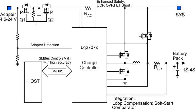
Simplified Schematic

4 Revision History
Changes from B Revision (March 2011) to C Revision
- Added ESD Ratings table, Feature Description section, Device Functional Modes, Application and Implementation section, Power Supply Recommendations section, Layout section, Device and Documentation Support section, and Mechanical, Packaging, and Orderable Information sectionGo
Changes from A Revision (November 2010) to B Revision
- Added Features for the bq24707 and bq24707A Go
- Added device bq24707A to this data sheetGo
- Added bq24707A to the ORDERING INFORMATION tableGo
- Added the COMPARISON TABLEGo
- Added bq24707 only to the test condition of tACOK_FALL_DEG first rowGo
- Added bq24707A only to the test condition of tACOK_FALL_DEG second rowGo
- Added (bq24707) to the title of Figure 2Go
- Added a new paragraph in the Battery Over Voltage Protection (BATOVP) sectionGo
- Changed the Description of the ACOK Deglitch Time Adjust bit in Table 3Go
- Changed the Adapter Detect and ACOK Output section. included 1.3s for bq24707 and 1.2ms for bq24707AGo
- Changed the Description of item U1 in Table 9Go
Changes from * Revision (July 2010) to A Revision